
Boron: Light-induced Degradation, Doping Role, Doping Concentration, Emitter Use, Safety and Sources, Degradation Fixes, Diffusion Sources, Resistivity, Physical Properties, Purity Control
Boron is a metalloid element with atomic number five, widely used as a p-type dopant in crystalline silicon. Key aspects include doping role, light-induced degradation, emitter use, doping concentration, degradation fixes, safety and sources, resistivity, diffusion sources, purity control, and physical properties. In a silicon wafer, boron atoms replace some silicon atoms and leave electron vacancies called holes, which makes the wafer positively charged in character and sets up the junction that separates charge. The amount of boron added, known as the doping concentration, shapes the wafer’s resistivity, its voltage output and how long charge carriers survive. When boron combines with oxygen in the wafer, sunlight can trigger light-induced degradation, which lowers cell efficiency during the first hours of exposure. Manufacturers limit this loss with gallium-doped wafers, lower oxygen content and regeneration treatments using heat and light. Boron also forms the emitter in n-type cells, and that layer feeds current into the wiring that carries solar panel DC power to the inverter.
Key Takeaways
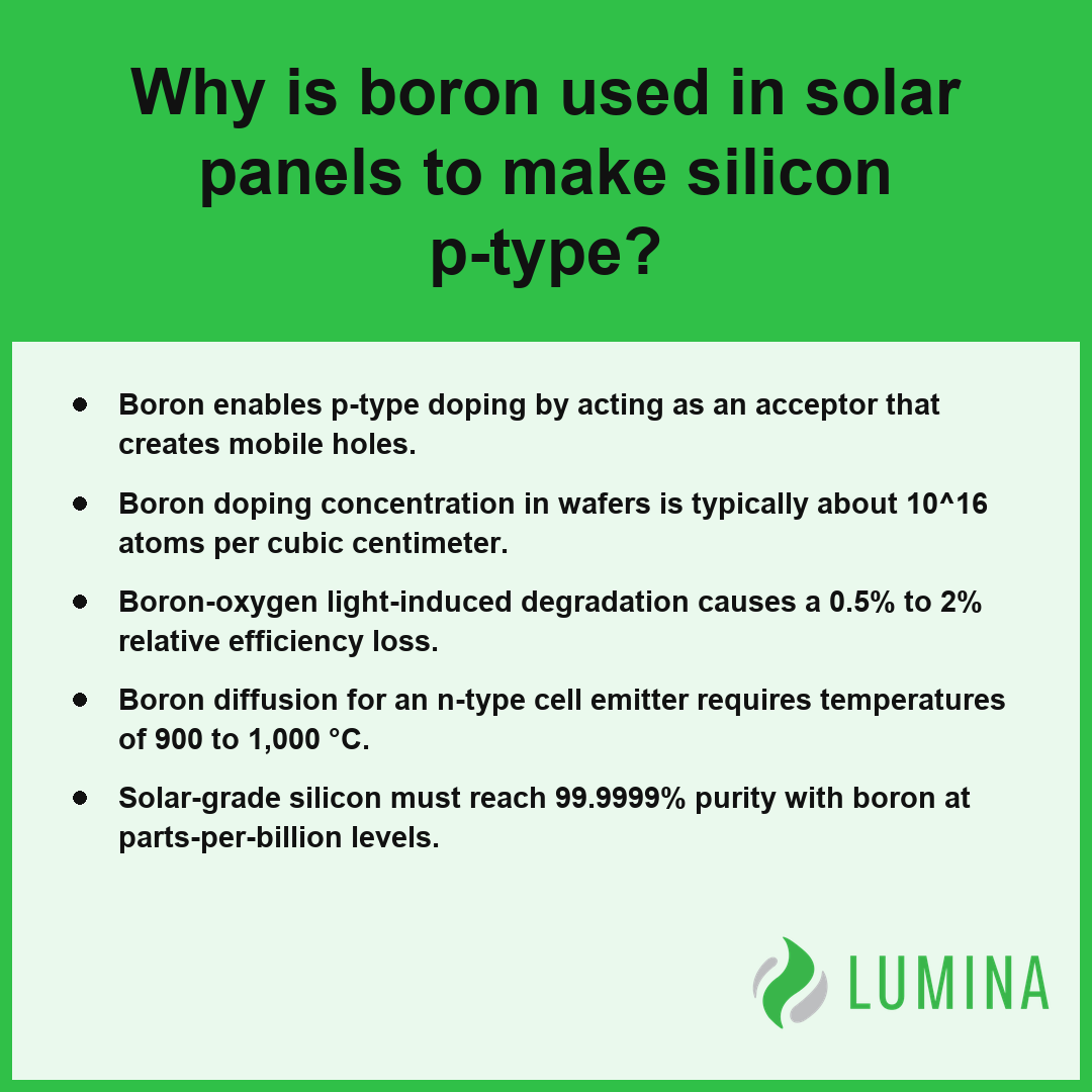
- Boron enables p-type doping by acting as an acceptor that creates mobile holes.
- Boron doping concentration in wafers is typically about 10^16 atoms per cubic centimeter.
- Boron-oxygen light-induced degradation causes a 0.5% to 2% relative efficiency loss.
- Boron diffusion for an n-type cell emitter requires temperatures of 900 to 1,000 °C.
- Solar-grade silicon must reach 99.9999% purity with boron at parts-per-billion levels.
Why Is Boron Used in Solar Panels to Make Silicon p-Type?
Boron is used in solar panels to make silicon p-type because it acts as an acceptor, introducing electron vacancies known as holes into the crystal lattice to facilitate positive charge transport. According to the Department of Energy, boron serves as a critical dopant in silicon-based solar cells to create a p-type layer by introducing a deficiency of electrons, which facilitates the formation of a positive charge carrier or hole. As an element with three valence electrons, boron creates these holes when it substitutes for a silicon atom in the structure, establishing the necessary conditions for p-type doping within a crystalline silicon solar cell.
| Property Parameter | Operational Metric | Doping Impact |
|---|---|---|
| Atomic Mass | 10.81 u | Substitution into silicon lattice |
| Segregation Coefficient | 0.8 | Influences concentration control in molten silicon |
| Target Resistivity | 0.5 – 3 ohm-cm | Optimizes electrical conductivity |
| Doping Concentration | 10^16 atoms/cm³ | Facilitates p-type hole formation |
| Thermal Stability | 2,076 °C | Ensures crystalline structural integrity |
Boron Technical Specifications
The technical implementation of this doping process relies on the specific physical properties of the material to ensure the wafer functions efficiently within a circuit. Key characteristics of using boron in this capacity include:
- Atomic mass of approximately 10.81 u.
- Typical wafer resistivity maintained between 0.5 to 3 ohm-cm.
- Doping concentrations targeted at about 10^16 atoms per cubic centimeter.
- High thermal stability with a crystalline melting point of around 2,076 °C.
Because boron is difficult to remove from molten silicon due to its segregation coefficient of about 0.8, manufacturers must carefully manage its concentration during the initial production of solar-grade silicon. Maintaining a purity level of 99.9999% (6N) or higher is essential to prevent unwanted electrical interference from stray impurities.
Review the technical specifications of your silicon wafers to verify that the target resistivity falls within the optimal range for your specific cell design.
The manufacturing process involves several critical steps to ensure effective integration of boron into the silicon substrate:- Czochralski process growth to pull single-crystal silicon ingots from the boron-doped melt.
- Wafer slicing using diamond wire saws to achieve precise thickness and surface finish.
- Chemical etching to remove surface damage and prepare the lattice for final processing.
- Surface passivation to minimize electron-hole recombination at the silicon interface.
How Much Boron Is in a Silicon Solar Wafer?
The amount of boron in a silicon solar wafer typically involves a doping concentration of about 10^16 atoms per cubic centimeter, which equates to roughly one boron atom for every few million silicon atoms. Because the physical properties of silicon are sensitive to impurities, this precise ratio is necessary to achieve the desired resistivity of 0.5 to 3 ohm-cm. Manufacturers must maintain these specific levels throughout the production of solar-grade silicon, as boron is notoriously difficult to remove from the silicon melt due to a segregation coefficient of about 0.8. According to the American Physical Society, the addition of boron to high-purity silicon serves as a foundational step to establish the positive charge carrier density required for the operation of the p-n junction in standard crystalline silicon photovoltaic cells.
| Material Characteristic | Specification Parameter | Operational Significance |
|---|---|---|
| Doping Concentration | ~10^16 atoms/cm³ | Establishes required p-type carrier density |
| Electrical Resistivity | 0.5 – 3.0 ohm-cm | Optimizes charge collection efficiency |
| Impurity Segregation | Coefficient of 0.8 | Governs difficulty of removal during melt |
| Base Material Purity | ≥ 99.9999% (6N) | Ensures semiconductor grade performance |
| Dopant Atomic Mass | 10.81 u | Physical constant of boron additive |
Target Resistivity Range (ohm-cm)
When you examine the material specifications for standard p-type wafers, the primary characteristics driven by boron content are defined as follows:
- Doping concentration: Approximately 10^16 atoms per cubic centimeter.
- Target resistivity: A range of 0.5 to 3 ohm-cm for optimal charge collection.
- Purity threshold: Solar-grade silicon must reach 99.9999% (6N) purity or higher, with boron held at parts-per-billion levels.
- Atomic mass: 10.81 u.
Monitoring the uniformity of boron distribution across the surface of the wafer is critical to ensuring your solar cells maintain consistent electrical performance across the entire module area.
To ensure the stability and performance of boron-doped silicon wafers, manufacturers must adhere to these additional processing considerations:- Maintain a high-purity argon atmosphere during the Czochralski crystal growth process to prevent oxygen contamination.
- Monitor the pulling rate of the silicon ingot to stabilize the uniform distribution of boron across the radial cross-section.
- Implement chemical mechanical polishing (CMP) to remove surface defects introduced during the wafer slicing process.
- Perform thermal annealing to neutralize structural lattice strain caused by the inclusion of boron atoms.
Does Boron Cause Solar Panels to Lose Efficiency in Sunlight?
Yes, boron causes a crystalline silicon solar cell to lose efficiency because the interaction between boron and oxygen within the wafer leads to boron-oxygen light-induced degradation, typically resulting in a relative efficiency loss of about 0.5% to 2% during the first hours to days of sunlight exposure.
| Degradation Characteristic | Scientific Mechanism | Impact on Photovoltaic Performance |
|---|---|---|
| Boron-Oxygen Complex Formation | Interaction of interstitial oxygen with p-type boron dopants | Creates recombination centers that trap charge carriers |
| Light-Induced Activation | Injection of excess charge carriers under solar illumination | Initial drop in conversion efficiency (0.5% to 2% relative) |
| Temporal Stability | Defect concentration equilibrium reached during initial exposure | Efficiency stabilizes after the first hours to days of sunlight |
Relative Efficiency Loss Range (%)
What Triggers Boron-Oxygen Light-Induced Degradation?
Boron-oxygen light-induced degradation occurs when boron atoms in the silicon crystal lattice interact with interstitial oxygen atoms under illumination. According to the National Renewable Energy Laboratory, the boron-oxygen complexes formed during the manufacturing of p-type Czochralski-grown silicon solar cells contribute to this light-induced degradation, which reduces cell efficiency when exposed to sunlight. These elements form complexes that act as recombination centers, capturing charge carriers before they can contribute to electrical current. The presence of oxygen is an inherent byproduct of standard silicon production methods, and when combined with boron, these light-sensitive defects emerge.
Why the Loss Appears in the First Hours to Days
The formation of these recombination centers is driven by the injection of excess charge carriers into the wafer when exposed to sunlight. This process is most active during the initial period of field exposure as the defects reach a stable concentration. You can observe the impact of this reaction through several chemical and physical variables:
- Boron doping concentration near 10^16 atoms per cubic centimeter
- Oxygen content inherent in Czochralski-grown silicon
- Intensity of incoming solar radiation
- Presence of hydrogen used during cell passivation
How Large Is the Efficiency Loss?
Yes, boron causes solar panels to lose efficiency in sunlight, with a typical relative efficiency loss from boron-oxygen light-induced degradation of about 0.5% to 2% within the first hours to days of exposure. This represents a performance drop that occurs shortly after the system is energized, as the internal atomic structure adjusts to the presence of high-intensity light.
Does the Loss Continue Over the Panel’s Lifetime?
No, the loss does not continue to increase indefinitely over the panel’s lifetime, as the degradation typically stabilizes once the boron-oxygen complexes reach a saturation point. Once this equilibrium is established, the panel maintains a steady performance level for the remainder of its operational cycle. Compare the initial degradation rate against the long-term stabilization data provided in your module’s technical specifications before finalizing your energy yield estimates.
Mitigation strategies for boron-oxygen defects in silicon manufacturing include the following approaches:- Switching to n-type silicon wafers, which utilize phosphorus instead of boron and are inherently resistant to this specific degradation mechanism.
- Utilizing Magnetic Czochralski (MCZ) growth processes to minimize oxygen content within the silicon crystal lattice.
- Applying thermal dark annealing or controlled hydrogen passivation treatments to neutralize the electrical activity of the defects.
- Deploying gallium-doped p-type wafers, which do not form the same efficiency-robbing complexes as boron-doped variants.
Preventing Boron-Oxygen Degradation and Comparing Gallium Doping as an Alternative
Preventing boron-oxygen light-induced degradation involves mitigating the specific interaction between interstitial boron and dissolved oxygen within the crystalline silicon solar cell lattice. While manufacturers can utilize chemical treatments like hydrogen passivation or regeneration processes to stabilize the wafer, gallium doping serves as a primary material-based alternative to avoid the mechanism entirely. According to the Solar Energy Industries Association, manufacturers in the United States have increasingly transitioned to gallium-doped monocrystalline silicon wafers to improve the long-term power output stability of solar modules.
Estimated Relative Efficiency Loss After Light Exposure
| Comparison Metric | Boron Doping | Gallium Doping |
|---|---|---|
| Primary Interaction | Forms degradation complexes with oxygen | Chemically stable against oxygen |
| Initial Efficiency | High, but subject to 0.5% to 2% relative loss | Stable under prolonged sunlight |
| Material Availability | Abundant and industry standard | Higher cost and sourcing complexity |
The choice between these dopants centers on a trade-off between the widespread processing infrastructure optimized for boron and the performance reliability offered by gallium. Because boron has a segregation coefficient of about 0.8, it remains difficult to refine from solar-grade silicon during directional solidification, making the adoption of gallium or high-purity n-type silicon a significant engineering decision for long-term module durability. Evaluate the anticipated environmental temperature profile of your installation, as high-heat climates can accelerate the reaction rates of lingering impurities in the silicon lattice.
Adopting gallium-doped silicon requires several adjustments to existing manufacturing workflows and material logistics:- recalibrating furnace pull speeds to compensate for gallium’s distinct segregation coefficient compared to boron.
- adjusting ingot slicing and wafer etching processes to accommodate the slightly different electronic properties of gallium-doped material.
- securing stable long-term supply chain agreements to offset the higher market price and lower historical availability of gallium.
- modifying quality control inspection protocols to account for the absence of light-induced degradation signatures during initial testing.
How Boron Is Used in the Emitter of TOPCon and Heterojunction Solar Cells
Boron is used in the emitter of TOPCon and heterojunction solar cells by creating a heavily doped p+ layer that effectively captures holes and facilitates charge separation at the junction. While boron-doped p-type silicon has historically formed the bulk of traditional cells, these advanced designs utilize boron diffusion to engineer the specific electronic properties of the emitter layer on n-type silicon substrates. Per Massachusetts Institute of Technology, boron-doped emitter layers are essential for creating the selective contact structures in high-efficiency heterojunction solar cells, which utilize thin amorphous silicon layers to passivate the crystalline silicon surface and minimize energy losses. By introducing boron atoms into the surface of the wafer at precise temperatures, manufacturers create a high-density region that helps minimize surface recombination and maximizes the collection of carriers generated by sunlight.
| Parameter | Specification / Detail | Functional Role in Cell Architecture |
|---|---|---|
| Primary Dopant Source | Boron Tribromide (BBr3) | Facilitates chemical vapor deposition of boron atoms into the n-type wafer surface. |
| Thermal Process Window | 900 °C – 1,000 °C | Ensures substitutional incorporation of boron atoms into the crystalline lattice. |
| Electronic Junction Type | p+ Emitter Region | Creates built-in potential to drive hole capture and charge separation. |
| Recombination Mitigation | Surface Passivation | Minimizes energy loss at the interface through high-density doping. |
Typical Boron Diffusion Temperature Range (°C)
- Boron tribromide (BBr3): The primary gaseous source used to introduce boron into the silicon surface via high-temperature deposition.
- Temperature range: The process requires a diffusion environment of roughly 900 to 1,000 °C to ensure the boron atoms substitute correctly into the crystal lattice.
- Carrier concentration: This diffusion forms a p+ region with a significantly higher doping density than the bulk, essential for establishing the required built-in potential.
- Material sources: Alternative delivery methods include boron trichloride (BCl3) or specialized boron-containing pastes applied prior to the diffusion cycle.
Review the specific sheet resistance targets provided by the cell manufacturer to determine if the boron diffusion depth is optimized for your target light-to-electricity conversion efficiency.
Key technical considerations for implementing boron diffusion in industrial cell manufacturing include:- Gas Phase Control: Precise regulation of oxygen flow during BBr3 delivery to manage the growth of the borosilicate glass layer.
- Etching Requirements: Post-diffusion removal of the boron-rich layer using hydrofluoric acid to prevent shunting and reduce contact resistance.
- Uniformity Management: Implementation of multi-zone furnace heating profiles to ensure consistent sheet resistance across large-area silicon wafers.
- Oxidation Cycles: Integration of short drive-in oxidation steps to stabilize the surface concentration and improve passivation quality.
Frequently Asked Questions
What resistivity should a boron-doped solar wafer have?
A boron-doped solar wafer should have a typical resistivity of 0.5 to 3 ohm-cm. This specific range is critical for defining how well the crystalline silicon solar cell conducts current and collects charge during operation, maintaining the intended electrical performance within the solar wafer.
What is the difference between BBr3, BCl3 and boron paste for boron diffusion in solar cell manufacturing?
Boron tribromide (BBr3), boron trichloride (BCl3), and boron-containing pastes are different material sources used for boron diffusion to form a p+ emitter at temperatures of 900 to 1,000 °C. These sources provide the necessary atoms to establish the electrical junction within the crystalline silicon solar cell.
Why is boron so hard to remove from solar-grade silicon?
Boron is difficult to remove from solar-grade silicon because its segregation coefficient is about 0.8, which makes directional solidification ineffective for purification. Because solar-grade silicon requires a purity of 99.9999% (6N) or higher, this property makes achieving the necessary parts-per-billion levels of concentration quite challenging.
What are the physical properties of boron, and do they matter for solar panels?
Crystalline boron has an atomic mass of about 10.81 u and a melting point around 2,076 °C. These properties are less critical than its role as an acceptor, which allows it to tune electrical behavior in silicon by creating holes through p-type doping, rather than generating power itself.
Is boron in solar panels safe, and where does the boron come from?
Boron is safely used in solar panels and borosilicate glass, originating from industrial sources like boron tribromide (BBr3) used in manufacturing. It functions as a dopant to manage electrical conductivity in crystalline silicon solar cells, and its presence is vital for the precise engineering of modern solar-grade silicon components.