
Cadmium Telluride: Safety, Efficiency, Heat Performance, Lifespan, Applications, Recycling, Manufacturing, Layer Structure, Material Supply, Environmental Footprint
Cadmium telluride is a crystalline compound of cadmium and tellurium used as the light-absorbing layer in thin-film photovoltaic modules. Key aspects include efficiency, safety, lifespan, heat performance, recycling, applications, layer structure, manufacturing, environmental footprint, and material supply. In a panel, a thin layer of this semiconductor sits between conductive coatings on glass, and sunlight knocking electrons loose in it produces direct current. It is the most widely produced thin-film technology, and many large solar companies use it in utility-scale arrays, where its low manufacturing cost and steady output matter. You will find that this article explains how efficient these modules are, how the cadmium content is contained and what that means for safety, and how long the panels typically last. It also covers how they behave in high temperatures and how recycling recovers the semiconductor material for reuse.
Key Takeaways
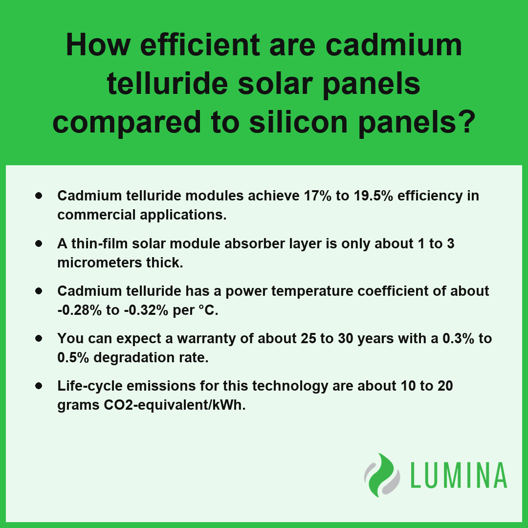
- Cadmium telluride modules achieve 17% to 19.5% efficiency in commercial applications.
- A thin-film solar module absorber layer is only about 1 to 3 micrometers thick.
- Cadmium telluride has a power temperature coefficient of about -0.28% to -0.32% per °C.
- You can expect a warranty of about 25 to 30 years with a 0.3% to 0.5% degradation rate.
- Life-cycle emissions for this technology are about 10 to 20 grams CO2-equivalent/kWh.
How Efficient Are Cadmium Telluride Solar Panels Compared to Crystalline Silicon?
Cadmium telluride solar panels offer an efficiency profile that, while slightly lower than the highest-performing crystalline silicon counterparts, provides a highly competitive alternative for utility-scale applications.
| Material Characteristic | Cadmium Telluride (CdTe) | Crystalline Silicon (c-Si) |
|---|---|---|
| Commercial Efficiency Range | 17% – 19.5% | 20% – 23% |
| Record Lab Efficiency | 22% – 23% | Higher (Industry Benchmark) |
| Absorber/Wafer Thickness | 1 – 3 micrometers | 150 – 200 micrometers |
| Band Gap Energy | ~1.45 eV (Direct) | ~1.12 eV (Indirect) |
Solar Module Efficiency Comparison
Commercial Module Efficiency Versus Laboratory Records
You will find a gap between the best performance seen in controlled settings and what you can buy for your project. While laboratory cells have achieved between 22% and 23% efficiency, commercial cadmium telluride thin-film solar modules generally reach about 17% to 19.5% efficiency. Per the Department of Energy, commercial cadmium telluride modules typically demonstrate power conversion efficiencies ranging between 17% and 19%, while standard commercial crystalline silicon panels generally occupy a slightly higher efficiency bracket of 20% to 23%. These figures reflect the scaling of production processes where large-area glass substrates are coated in high-speed manufacturing environments.
Why Does Absorber Layer Thickness Matter for Efficiency?
How the Band Gap Shapes Light Absorption
The efficiency of your system is directly tied to the unique physical properties of the semiconductor used. Cadmium telluride features a direct band gap of about 1.45 eV, which allows for near-ideal capture of the solar spectrum within an extremely thin profile.
- Absorber layer thickness: 1 to 3 micrometers
- Crystalline silicon wafer thickness: 150 to 200 micrometers
- Optical absorption: Over 90% of above-gap photons captured in the thin layer
Because of this strong absorption coefficient, you require significantly less material to convert sunlight into electricity, which helps reduce the overall energy payback time for the system.
Where Crystalline Silicon Still Leads
Crystalline silicon currently maintains a higher top-tier efficiency ceiling for individual modules, often exceeding the 20% mark in premium commercial products. If your installation footprint is extremely limited, the higher power density of silicon may offer a space-saving advantage over thin-film technology.
Evaluate your available land area versus the total energy output needs to determine if you require the higher power density of silicon or the utility-scale cost efficiency of cadmium telluride.
Several technical factors contribute to the efficiency variance observed between laboratory prototypes and mass-produced thin-film modules:- Substrate Uniformity: Maintaining consistent semiconductor deposition across large-area glass sheets is more complex than in small-scale laboratory coating processes.
- Edge Recombination: The physical connections and laser-scribing required to interconnect individual cells on a module can introduce localized resistive losses.
- Spectral Response: Commercial modules must be optimized for a broad range of real-world solar incidence angles and temperatures, which can necessitate trade-offs compared to peak-performance lab conditions.
- Manufacturing Speed: High-throughput manufacturing environments prioritize production velocity, which may lead to minor crystalline defects that would be avoided in slower, controlled lab synthesis.
Is Cadmium Telluride in Solar Panels Safe Given That Cadmium Is Toxic?
Yes, cadmium telluride is safe in solar panels because the toxic cadmium is chemically bound into a stable compound, preventing it from leaching into the environment during normal use. Per the National Renewable Energy Laboratory, cadmium telluride is chemically stable and bound in a solid-state crystal lattice, which prevents the release of cadmium during standard solar panel operation and environmental exposure. While elemental cadmium is hazardous, cadmium telluride is a crystalline compound with a high melting point of about 1,041 °C, which ensures it remains solid under all operational and extreme environmental conditions. The material is safely trapped through the encapsulation process, where it is hermetically sealed between layers of glass, effectively isolating the semiconductor from contact with the atmosphere or water.
| Hazard Mitigation Factor | Physical Property | Safety Benefit |
|---|---|---|
| Molecular Stability | Solid-state crystal lattice | Prevents cadmium leaching into water or soil |
| Thermal Integrity | 1,041 °C melting point | Prevents vaporization during fires or extreme heat |
| Structural Sealing | Hermetic glass-on-glass encapsulation | Isolates material from atmospheric contact |
| Chemical Reactivity | Inert semiconductor state | Eliminates interaction with external environmental elements |
| Solubility Resistance | Water-insoluble compound | Prevents runoff contamination if modules are damaged |
Safety in these modules is maintained by several design characteristics that prevent human or environmental exposure:
- The stable crystalline structure prevents the compound from dissolving in water, which eliminates the risk of runoff if glass is cracked.
- The high melting point ensures that the material does not vaporize or migrate under standard operating temperatures or even in high-heat fire scenarios.
- Robust glass-on-glass encapsulation keeps the internal components secure throughout the entire operational life of the thin-film solar module.
- The manufacturing process creates a chemically inert semiconductor layer that does not easily interact with its surroundings.
Compare the specific hazardous material handling protocols provided by different manufacturers to understand how they manage panel integrity during installation and potential physical impact events.
In addition to these material properties, the industry follows specific protocols to ensure the safety of cadmium telluride modules throughout their life cycle:- Manufacturers operate comprehensive take-back and recycling programs to ensure modules are recovered at the end of their service life rather than entering waste streams.
- Advanced shredding and chemical leaching processes are used in recycling facilities to safely separate the semiconductor material from the glass and frame components.
- Life-cycle assessments consistently demonstrate that the environmental footprint of managing these panels is significantly lower than the emissions saved by the clean energy they produce.
- Regulatory compliance standards, such as the Restriction of Hazardous Substances (RoHS) directive, mandate strict reporting and handling procedures for materials containing cadmium compounds.
How Long Cadmium Telluride Solar Panels Last and How Fast They Degrade
Cadmium telluride solar panels last for a standard operational service life typically ranging from about 25 to 30 years before their power output falls significantly below initial rated levels. This longevity is supported by robust glass-based encapsulation that protects the internal semiconductor layers from moisture and atmospheric pollutants, ensuring the electrical integrity of the heterojunction over decades of exposure to outdoor elements. Throughout this period, you can expect a consistent performance decline, which is quantified by an annual degradation rate of around 0.3% to 0.5% per year.
| Performance Metric | Minimum Value | Maximum Value |
|---|---|---|
| Operational Service Life (Years) | 25 | 30 |
| Annual Power Degradation Rate (%) | 0.3% | 0.5% |
| Semiconductor Melting Point (°C) | 1,041 °C | |
Estimated Annual Degradation Rate (%)
Several factors contribute to the predictable longevity and stability of cadmium telluride systems in the field:
- High material stability: The crystalline compound features a high melting point of about 1,041 °C, which prevents internal layer migration or structural instability under common operating temperatures. Per the United States Department of Energy, this thin-film technology demonstrates high stability and resistance to thermal stress, which contributes to long-term performance reliability in diverse climate zones.
- Durable packaging: The use of glass superstrates and back contacts provides a rigid barrier against physical stress and environmental ingress.
- Low degradation mechanics: The specific semiconductor chemistry minimizes the chemical instability often associated with other thin-film technologies, maintaining voltage and current output stability.
When assessing a potential system, review the specific degradation performance data in the manufacturer warranty documentation to see how the annual output decline aligns with your site’s environmental conditions.
Several environmental and design features further enhance the reliability of these solar modules:- Secondary containment layers utilize specialized sealants to prevent edge corrosion caused by humidity ingress.
- The monolithic manufacturing process eliminates individual cell interconnects, reducing potential failure points from mechanical vibration or thermal expansion.
- Glass-on-glass laminate construction provides high mechanical strength, protecting the thin-film layer from physical damage during extreme weather events like hail or high winds.
- The specific molecular structure of the semiconductor naturally resists light-induced degradation, maintaining structural cohesion over extended ultraviolet exposure.
Heat Performance: Cadmium Telluride Versus Crystalline Silicon in Hot Climates
Heat performance for cadmium telluride compared to crystalline silicon is superior in hot climates because of its physical properties. When solar modules operate in high-temperature environments, their ability to convert sunlight into electricity typically declines, but CdTe technology minimizes these losses more effectively than its silicon counterparts. Lawrence Berkeley National Laboratory reports that thin-film cadmium telluride technology maintains a more stable power output in high-heat environments compared to standard crystalline silicon modules, which typically face greater voltage losses under elevated thermal conditions. This advantage stems from a lower power temperature coefficient, allowing the material to maintain a higher portion of its rated output as ambient and cell temperatures rise.
| Thermal Performance Metric | Cadmium Telluride (CdTe) | Crystalline Silicon (c-Si) |
|---|---|---|
| Power Temperature Coefficient | -0.28% to -0.32% / °C | -0.40% to -0.50% / °C |
| High-Heat Voltage Retention | High (Superior Stability) | Moderate (Increased Loss) |
| Diffuse Light/Humidity Response | Optimized Efficiency | Standard Efficiency |
| Thermal Dissipation Profile | Thin-Film Efficiency | Wafer-Based Resistance |
| Energy Payback Time | Under 1 Year | 1 to 2 Years (Industry Average) |
Power Temperature Coefficient Comparison (% per °C)
Note: Standard crystalline silicon typically ranges from -0.40% to -0.50% per °C; midpoint used for comparison.
- Power temperature coefficient for CdTe: about -0.28% to -0.32% per °C.
- Superior performance in diffuse light and high humidity, which often accompany hot, tropical, or summer conditions.
- Reduced thermal stress on internal components, as the thin-film solar module structure dissipates heat differently than standard crystalline silicon wafers.
- Lower energy payback time, often under one year, ensuring that operational efficiency gains in high-heat zones translate quickly into net carbon reductions.
Evaluate the temperature coefficient of specific module models when planning for utility-scale arrays in regions where ambient temperatures frequently exceed 30 °C.
Additional operational benefits of cadmium telluride thin-film technology include the following environmental and structural advantages:- Reduced material shadow loss during partial shading due to the monolithically integrated cell structure.
- Lower susceptibility to micro-cracking often caused by thermal expansion stress in rigid wafer-based panels.
- Enhanced performance in high-humidity climates owing to superior glass-on-glass packaging durability.
- Lower life-cycle carbon footprint attributed to a shorter manufacturing process compared to energy-intensive silicon purification.
What Happens to Cadmium Telluride Solar Panels at End of Life and How Recycling Works
End-of-life recycling for cadmium telluride solar panels ensures that valuable materials are recovered while managing the compound’s stable structure to prevent environmental release. Because cadmium telluride is manufactured using high-speed deposition methods that coat glass with a thin absorber layer, the recycling process focuses on separating these conductive and semiconductor materials from the glass superstrate, which constitutes the vast majority of the module’s mass. Per the Environmental Protection Agency, cadmium telluride panels fall under the federal Resource Conservation and Recovery Act, requiring owners to ensure they are managed as hazardous waste unless they meet specific state-level regulatory exemptions.
| Recycling Phase | Primary Material Target | Technical Objective |
|---|---|---|
| Mechanical Shredding | Glass Superstrate | De-encapsulation of thin-film layers |
| Material Separation | Conductive Coatings | Isolation of semiconductor residues from substrate |
| Chemical Leaching | Cadmium & Tellurium | Solubilization of semiconductor compounds |
| Purification & Refinement | Raw Semiconductor Feedstock | Closed-loop grade restoration for manufacturing |
- Mechanical shredding: The thin-film solar module is crushed into smaller fragments to break the bond between the glass and the encapsulated materials.
- Material separation: Through specialized screening and washing processes, the glass fragments are separated from the semiconductor residues and conductive coatings.
- Chemical leaching: The semiconductor material, containing cadmium and tellurium, is treated to dissolve the compounds, allowing them to be extracted from the waste stream.
- Purification and refinement: The recovered cadmium and tellurium are purified to reach the high grades required to manufacture new cadmium telluride cells, creating a closed-loop system for the supply chain.
Confirm that your project developer or service provider has a verified retrieval program in place that guarantees the recovery of these processed materials rather than simple disposal.
The recycling workflow utilizes specific technical methods to optimize material recovery and environmental safety:- Centrifugal milling: Used to further pulverize glass fragments, ensuring the thin-film semiconductors are fully detached from the substrate surfaces.
- Magnetic separation: Employs high-strength magnets to remove any metallic connectors or structural frame components before chemical processing.
- Ion exchange: A secondary refinement step that captures dissolved metallic ions from leaching fluids to improve overall recovery efficiency.
- Thermal treatment: Applied in controlled atmospheres to volatilize organic contaminants or ethylene vinyl acetate (EVA) encapsulants.
Frequently Asked Questions
What layers make up a cadmium telluride solar cell and what does each one do?
A cadmium telluride solar cell consists of a glass superstrate, a transparent conductive oxide, an n-type buffer layer like cadmium sulfide, a p-type CdTe absorber layer, and a back contact. This structure forms a heterojunction that allows the cell to convert sunlight into electricity efficiently within a thin profile.
How are cadmium telluride solar panels manufactured?
Cadmium telluride thin-film solar modules are manufactured using high-speed deposition methods such as close-space sublimation and vapor transport deposition. These processes coat glass substrates at temperatures around 500 to 600 °C, creating a high-performance absorber layer in just minutes to form a complete, durable solar module for commercial use.
Why are cadmium telluride solar panels used in solar farms but rarely on residential roofs?
Cadmium telluride solar panels are primarily used in utility-scale arrays because they are optimized for large-format, high-speed production. While they offer excellent performance in hot climates due to a low power temperature coefficient of about -0.28% to -0.32% per °C, their large surface area is specifically engineered for industrial-scale deployment.
What is the carbon footprint and energy payback time of cadmium telluride solar panels?
The life-cycle carbon footprint of cadmium telluride is about 10 to 20 grams CO2-equivalent per kWh, and its energy payback time is often under one year in sunny locations. This makes the technology one of the most sustainable options available, boasting high energy efficiency with a minimal environmental impact.
Is there enough tellurium to scale up cadmium telluride solar panel production?
Yes, there is enough tellurium to scale up production, as cadmium telluride remains the second most deployed photovoltaic material globally. Manufacturers continue to increase capacity for these thin-film solar modules, utilizing the material’s strong light absorption to create efficient, cost-effective energy solutions despite the specific constraints of raw material supply.