
Perovskite Solar Cell: Lifespan, Efficiency, Availability, Price, Formats, Toxicity, Layer Structure, Materials, Manufacturing, Bandgap

A perovskite solar cell is a photovoltaic device that uses a perovskite-structured compound as its light-absorbing layer. Key aspects include efficiency, lifespan, price, availability, toxicity, formats, materials, layer structure, bandgap, and manufacturing. Light striking the perovskite layer frees electrons, and thin charge-transport layers on either side guide them into an electrical current. Within solar panels, this technology is mainly seen as a lighter, cheaper-to-make alternative or partner to silicon, and it is often layered on top of silicon cells to capture more of the spectrum. If you are thinking about a solar installation PA, it helps to know that most rooftop systems still use silicon, while perovskite modules are only beginning to reach the market. The article goes on to explain efficiency, lifespan, price, availability and toxicity, including the lead content found in many perovskite compounds.
Key Takeaways
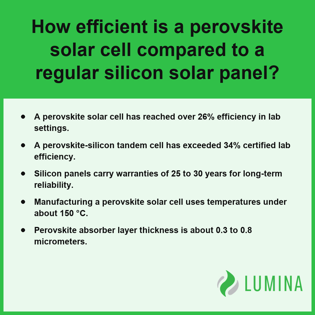
- A perovskite solar cell has reached over 26% efficiency in lab settings.
- A perovskite-silicon tandem cell has exceeded 34% certified lab efficiency.
- Silicon panels carry warranties of 25 to 30 years for long-term reliability.
- Manufacturing a perovskite solar cell uses temperatures under about 150 °C.
- Perovskite absorber layer thickness is about 0.3 to 0.8 micrometers.
How Efficient Is a Perovskite Solar Cell Compared to a Silicon Panel?
While a commercial silicon panel typically offers a module efficiency ranging from 20% to 24%, you can achieve significantly higher performance with a perovskite-silicon tandem cell, which has exceeded 34% certified lab efficiency, compared to a single-junction cell that has passed 26% lab efficiency.
| Cell Architecture | Status/Classification | Record Lab Efficiency | Performance Context |
|---|---|---|---|
| Commercial Silicon | Market Standard | 22% | Baseline for current rooftop installations |
| Single-Junction Perovskite | Emerging Tech | 26% | Rivals silicon with minimal material footprint |
| Single-Junction Silicon | Theoretical Limit | 29% | Shockley-Queisser constraint barrier |
| Perovskite-Silicon Tandem | High-Performance | >34% | Surpasses single-junction spectral constraints |
Solar Cell Efficiency Comparison (Lab)
Lab Efficiency of Single-Junction Cells
A perovskite solar cell reaches competitive efficiency levels quickly, with lab single-junction perovskite solar cell efficiency having passed 26%, which rivals the performance of established silicon technology. You benefit from this rapid progression because the perovskite absorber layer, typically only 0.3 to 0.8 micrometers thick, maintains high light absorption and long carrier diffusion lengths despite its minimal footprint.
Why Perovskite-Silicon Tandem Cells Score Higher
Yes, a perovskite-silicon tandem cell allows you to surpass the theoretical constraints of single-material designs by capturing a broader spectrum of light. National Renewable Energy Laboratory reports that perovskite-silicon tandem cells have achieved laboratory-scale power conversion efficiencies exceeding 33 percent, surpassing the theoretical Shockley-Queisser limit of approximately 29 percent for single-junction silicon-only panels. While single-junction silicon panels are generally limited to a practical ceiling of roughly 29% to 30%, these tandem devices have exceeded 34% certified lab efficiency.
How Bandgap Tuning Raises Efficiency
Efficiency gains rely on the ability to customize the material properties for specific light wavelengths. Because the bandgap is tunable from about 1.2 to 2.3 eV by changing halide mix and cations, researchers can optimize the top perovskite layer to absorb high-energy photons while letting lower-energy light pass through to the silicon base.
- Single-junction silicon: 20–24% module efficiency
- Single-junction perovskite: 15–20% module efficiency
- Perovskite-silicon tandem: 25–28% module efficiency
Does Lab Efficiency Carry Over to Module Efficiency?
Lab efficiency metrics often differ from real-world results due to the scaling challenges involved in transitioning from small-area cells to large-format modules. Although early production modules demonstrate that perovskite-silicon tandem cells hold significant promise for future installations, the current commercial landscape for silicon panels remains the benchmark for stable, field-tested performance.
Compare the anticipated conversion gain of a tandem product against the standard performance output of a traditional silicon panel before deciding if the extra efficiency justifies the investment.
The unique material properties of perovskites contribute to these performance breakthroughs through several distinct mechanisms:- Tunable bandgaps allow the material to be engineered to absorb specific segments of the solar spectrum, particularly high-energy photons.
- Solution-processing methods, such as spin coating or inkjet printing, significantly lower manufacturing energy requirements compared to high-heat silicon crystallization.
- Flexible substrate compatibility enables the integration of solar technology into lightweight, portable, or curved surfaces.
- Superior defect tolerance allows for high carrier mobility even in polycrystalline thin films, reducing the need for ultra-high-purity materials.
How Long a Perovskite Solar Cell Lasts Versus a 25-30 Year Silicon Warranty
The lifespan of a perovskite solar cell is currently shorter than the 25-30 year silicon warranty period, as the technology remains in an active phase of maturing its environmental resilience. According to the Department of Energy, while silicon-based panels typically maintain a 25 to 30-year performance warranty in the United States, commercial-scale perovskite cells remain in the research and development phase regarding their ability to withstand long-term environmental degradation over comparable timeframes. While a silicon panel relies on a stable, crystalline structure that has been field-tested for decades, a perovskite solar cell uses a perovskite absorber layer that is susceptible to degradation from external stressors. Without proper encapsulation, exposure to moisture, oxygen, and ultraviolet light can destabilize the crystal structure. Researchers utilize standardized benchmarks to measure progress toward long-term durability, such as the damp heat stability test under IEC 61215, which subjects modules to 85 °C and 85% humidity for 1,000 hours to simulate extreme environmental wear.
Manufacturing Process Temperature (°C)
| Factor | Silicon Panel | Perovskite Solar Cell |
|---|---|---|
| Warranty | 25 to 30 years | Emerging (Variable) |
| Primary Threat | Mechanical micro-cracks | Moisture and heat ingress |
| Manufacturing Heat | Over 1,000 °C | Under 150 °C |
To ensure a perovskite solar cell meets your expectations for longevity, verify the manufacturer’s specific environmental stress testing data beyond baseline industry requirements.
To ensure a perovskite solar cell meets your expectations for long-term reliability, consider the following integration and maintenance factors:- Implement advanced edge seals and multi-layer barrier encapsulation to prevent atmospheric ingress.
- Prioritize bifacial module configurations to minimize thermal buildup within the absorber layer.
- Utilize UV-filtering glass covers to mitigate photon-induced degradation of the crystal structure.
- Deploy integrated monitoring systems to track performance drops consistent with early-stage chemical instability.
What Drives the Cost Per Watt of Perovskite Solar Panels
The cost per watt of perovskite solar panels is primarily driven by lower raw material usage, reduced energy consumption during production, and the potential for high-throughput manufacturing methods. Because the perovskite absorber layer thickness is about 0.3 to 0.8 micrometers, versus about 150 to 180 micrometers for silicon wafers, you benefit from a drastically reduced physical requirement for semiconductors. Furthermore, the ability to perform solution processing or vapor deposition at film processing temperatures under about 150 °C, versus over 1,000 °C for silicon, allows for significant operational savings in energy expenditures.
| Manufacturing Metric | Perovskite Technology | Traditional Silicon |
|---|---|---|
| Absorber Layer Thickness | 0.3 – 0.8 micrometers | 150 – 180 micrometers |
| Thermal Processing Requirement | < 150 °C | > 1,000 °C |
| Production Methodology | Roll-to-roll / Solution-based | Batch-based wafer fabrication |
| Substrate Flexibility | High (Plastic/Flexible) | Low (Rigid Wafers) |
Manufacturing Process Temperature (°C)
- Reduced Material Mass: The thin-film nature of the perovskite absorber layer allows for massive reductions in raw material weight and cost compared to bulky silicon ingots. United States Department of Energy reports that the potential for utilizing abundant, low-cost raw materials in perovskite synthesis reduces dependency on the high-purity crystalline silicon supply chain.
- Low-Temperature Processing: Keeping production temperatures under 150 °C enables the use of flexible or plastic substrates, which can further lower logistics and mounting costs.
- High-Speed Manufacturing: Compatibility with roll-to-roll printing and slot-die coating processes facilitates continuous production flows that exceed the speed of batch-based silicon wafer fabrication.
- Integrated Versatility: The ability to manufacture a perovskite solar cell directly onto existing glass or flexible supports reduces the secondary structural components required for a finished module.
Compare the anticipated capacity factor of these panels against the total installation footprint to determine if the material savings justify the current production-scale trade-offs for your specific site.
Beyond material and thermal advantages, the manufacturing transition to perovskite solar technology offers several distinct operational benefits:- Reduced facility footprint requirements due to the replacement of high-heat vacuum chambers with compact, room-temperature printing equipment.
- Lower capital expenditure (CAPEX) enabled by the ability to utilize modular, continuous manufacturing lines instead of multi-stage batch processing.
- Increased potential for building-integrated photovoltaics (BIPV) through the use of lightweight, non-glass substrates.
- Enhanced scalability in geographic regions with limited access to specialized, high-energy-intensive industrial infrastructure.
Steps to Take If You Want Perovskite Solar Panels for Your Home Right Now
Steps to take if you want perovskite solar panels for your home right now focus primarily on identifying the limited commercial availability of these technologies, as they are still transitioning from specialized applications into the residential market. Because you cannot currently walk into a typical hardware retailer and buy a standard-sized perovskite module, you must look toward emerging thin-film suppliers or specific energy-innovation partnerships that are piloting these modules. Per Department of Energy, commercial adoption of this technology remains contingent on overcoming significant challenges related to long-term outdoor stability and moisture-induced degradation under real-world weather conditions.
| Reliability Metric | Standard Protocol | Industry Benchmark | Residential Expectation |
|---|---|---|---|
| Environmental Durability | IEC 61215 Damp Heat Test | 1,000 Hours @ 85°C/85% RH | Critical for Moisture Resistance |
| Operational Lifespan | Standard Silicon Warranty | 25 to 30 Years | Target for Tandem Stability |
| Material Integrity | Absorber Composition | Stability-Enhancing Halides | Required for Real-World Weathering |
| Commercial Availability | Market Transition Status | Pilot/Innovation Partnerships | Not Available at Retail |
Warranty and Test Durations (Hours/Years)
- Verify that your prospective installer offers perovskite-silicon tandem cell products, as pure single-junction modules for residential rooftops are not yet standard retail items.
- Confirm the encapsulation standards used for any perovskite solar cell you consider, ensuring the modules have been validated against the IEC 61215 damp heat test (85 °C and 85% humidity for 1,000 hours).
- Request documentation on the specific perovskite absorber layer composition to confirm it utilizes modern stability-enhancing halides rather than early-stage, moisture-sensitive compounds.
- Compare the manufacturer’s performance guarantees against the 25 to 30 year warranties typically provided with a silicon panel to account for potential gaps in long-term degradation data.
- Evaluate the mounting requirements for any lightweight or flexible perovskite-based products, which often necessitate different installation hardware than heavy, rigid silicon panels.
Investigate the specific degradation rate documentation provided by the manufacturer to understand how the power output of your chosen perovskite solar cell will be compensated if it drops below the promised threshold before the end of the expected service life.
To ensure your potential perovskite installation meets project viability requirements, follow these verification steps:- Request independent third-party certification reports to validate the module’s performance under accelerated stress testing.
- Confirm that the manufacturer provides a performance guarantee specifically covering tandem-cell efficiency degradation.
- Verify the specific encapsulation techniques used to mitigate lead leakage and moisture ingress in outdoor environments.
- Check local building codes and residential zoning requirements for thin-film material integration on existing rooftops.
Lead in a Perovskite Solar Cell: Toxicity Risks Compared by Exposure Point
Lead in a perovskite solar cell poses toxicity risks that are primarily determined by the physical state of the material and its potential for leakage throughout the product life cycle. Because the perovskite absorber layer utilizes lead halides, the risk of exposure is low during standard operation but becomes a factor during manufacturing, handling of damaged modules, and end-of-life disposal.
Perovskite Absorber Layer Thickness (micrometers)
| Exposure Point | Primary Risk Factor | Exposure Mechanism |
|---|---|---|
| Manufacturing | High (Industrial) | Inhalation of precursor dust or liquid solution aerosols |
| Standard Operation | Negligible | Encapsulation prevents lead leaching from the perovskite solar cell |
| Damage/Breakage | Moderate | Physical release of lead-containing fragments if seals fail |
| End-of-Life | High (Environmental) | Leaching into groundwater if not processed via controlled recycling |
The total lead content in a perovskite solar cell remains very low compared to traditional industrial sources due to the minimal thickness of the perovskite absorber layer, which measures only 0.3 to 0.8 micrometers. While this thin-film structure minimizes the absolute mass of lead required, the solubility of lead halides means that if the encapsulation layer is compromised, the material can potentially migrate if exposed to environmental moisture. Per the Environmental Protection Agency, materials containing lead are classified as hazardous waste under the Resource Conservation and Recovery Act if they fail the Toxicity Characteristic Leaching Procedure, which mandates rigorous containment and recycling procedures for discarded perovskite modules in the United States. You should verify the manufacturer’s specific protocols for module take-back and recycling programs to ensure that decommissioned units are handled as hazardous material rather than entering general waste streams.
To mitigate potential environmental and health impacts, the following management strategies are recommended for perovskite solar cell life cycle oversight:- Implement closed-loop manufacturing systems to capture particulate precursors before they exit the production environment.
- Apply hydrophobic encapsulation polymers to maintain material stability even when the module surface is breached.
- Establish dedicated take-back programs to ensure modules are directed to industrial smelting facilities rather than landfills.
- Utilize chemical chelating agents during the recycling process to stabilize and sequester lead ions before material recovery.
Frequently Asked Questions
What is a perovskite solar cell made of, and why is it called perovskite?
A perovskite solar cell is made of a light-absorbing layer with an ABX3 crystal structure, usually a hybrid organic-inorganic lead halide. The name originates from the mineral calcium titanate, discovered in 1839 and named for Lev Perovski; the solar material shares only this specific crystal structure with the original mineral.
What are the layers inside a perovskite solar cell and what does each one do?
A perovskite solar cell contains a transparent conductive glass base, an electron transport layer, a perovskite absorber layer, a hole transport layer, and a metal electrode. Photons create electron-hole pairs in the absorber layer, which the transport layers then separate and collect to generate current from the captured light energy.
How does bandgap tuning let a perovskite solar cell work as the top layer on a silicon tandem panel?
Bandgap tuning allows a perovskite solar cell to function as a top layer by adjusting its range from about 1.2 to 2.3 eV through changes in halide mix and cations. An optimal value of 1.65 to 1.7 eV captures high-energy light, letting lower-energy light pass through to the silicon layer.
How are perovskite solar cells manufactured, and why is it cheaper than making silicon?
Perovskite solar cells are manufactured using solution processing or vapor deposition at temperatures under about 150 °C, which is significantly lower than the over 1,000 °C required for silicon. Furthermore, the perovskite absorber layer thickness is only about 0.3 to 0.8 micrometers, requiring much less material than 150 to 180 micrometer silicon wafers.
What types of perovskite solar cells exist, such as flexible, semi-transparent window, and indoor low-light versions?
Available forms of this technology include rigid glass modules, flexible lightweight films, and semi-transparent cells suitable for windows. Researchers also develop all-perovskite tandem units and the high-efficiency perovskite-silicon tandem cell. Each variant utilizes the light-harvesting properties inherent to the specific composition and structure of each individual perovskite solar cell.