
Selenium: Efficiency, Role in Panels, Heat Performance, Toxicity, Forms, Recycling, Price, Bandgap, Emerging Alternatives, Supply
Selenium is a nonmetallic chemical element, atomic number 34, used as a semiconductor in some photovoltaic cells. Key aspects include role in panels, efficiency, toxicity, heat performance, recycling, forms, bandgap, price, supply, and emerging alternatives. In solar panels, selenium appears mainly in copper indium gallium selenide thin-film cells, where a thin layer absorbs sunlight and releases electrons to create current. It also played a historic part in the first photovoltaic devices of the 1880s, which converted light into electricity at very low efficiency. Information about local installation options, such as solar companies Washington, often mentions thin-film modules because they handle diffuse light and warm conditions differently from silicon. The article goes on to explain the role of selenium in panels, its efficiency, its heat performance, its toxicity, and how recycling recovers it.
Key Takeaways
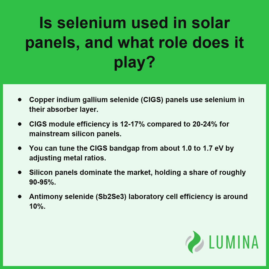
- Copper indium gallium selenide (CIGS) panels use selenium in their absorber layer.
- CIGS module efficiency is 12-17% compared to 20-24% for mainstream silicon panels.
- You can tune the CIGS bandgap from about 1.0 to 1.7 eV by adjusting metal ratios.
- Silicon panels dominate the market, holding a share of roughly 90-95%.
- Antimony selenide (Sb2Se3) laboratory cell efficiency is around 10%.
Is Selenium Used in Solar Panels, and What Role Does It Play?
Yes, selenium is used in solar panels as a fundamental material in specific thin-film technologies, primarily functioning as a key component of the semiconductor compound within the absorber layer.
| Material System | Role in Photovoltaics | Bandgap Range (eV) | Technological Significance |
|---|---|---|---|
| Copper Indium Gallium Selenide (CIGS) | Semiconductor Absorber Layer | 1.0 – 1.7 | High efficiency and mechanical flexibility |
| Gray Selenium | Original Light-to-Electricity Converter | ~1.7 | Foundational historical photovoltaic material |
| Antimony Selenide (Sb2Se3) | Emerging Thin-Film Component | ~1.1 – 1.2 | Low-cost alternative material architecture |
Bandgap Range of CIGS Solar Cells (eV)
Selenium in Copper Indium Gallium Selenide (CIGS) Absorber Layers
In copper indium gallium selenide (CIGS) technology, selenium acts as an essential binding element within the thin-film structure. The absorber layer, which typically measures 1-3 micrometers thick, relies on the chemical properties of selenium to create the necessary semiconductor lattice. This material is sourced as a byproduct of refining copper from anode slimes, with global production reaching about 3,000 metric tons per year. According to the National Renewable Energy Laboratory, selenium serves as a key component in these CIGS thin-film solar cells, which are notable for their high efficiency and flexibility when compared to standard crystalline silicon panels.
How Gallium-to-Indium Ratios Tune the Bandgap
You can adjust the electronic properties of the CIGS material by altering the ratio of gallium to indium. This precise tuning allows manufacturers to set the bandgap between about 1.0 and 1.7 eV, optimizing how much of the solar spectrum the panel captures.
Early Gray Selenium Cells and Emerging Antimony Selenide (Sb2Se3)
The history of photovoltaics began with gray selenium in the 1880s, which offered a simple form of light-to-electricity conversion. While those original devices achieved only 1% efficiency, research continues into new selenium-based materials:
- Antimony selenide (Sb2Se3): A promising thin-film material currently achieving laboratory cell efficiency of around 10%.
- Pure selenium cells: Experimental single-element devices currently reaching 5–8% laboratory efficiency.
Why Do Silicon Panels and Cadmium Telluride (CdTe) Panels Use Little or No Selenium?
Silicon panels dominate the market with a 90–95% share because they rely on crystalline silicon as the primary semiconductor, requiring no selenium for operation. Conversely, cadmium telluride (CdTe) panels utilize tellurium as their main absorber. While some CdTe designs incorporate small amounts of selenium to form a cadmium selenide telluride layer, it remains a minor additive rather than the primary substance.
Investigate the specific semiconductor composition listed on technical datasheets if you want to verify whether a particular thin-film product relies on selenium-based compounds for its energy conversion.
The production and application of selenium in solar energy involve several specialized industrial and chemical processes:- Selenium recovery is primarily achieved through the electrolytic refining of copper, where it is extracted from the accumulated anode slimes.
- The vacuum co-evaporation process is commonly utilized to deposit selenium alongside copper, indium, and gallium onto substrates to form the CIGS semiconductor film.
- Post-deposition annealing in a selenium-rich atmosphere is often required to ensure optimal crystallinity and reduce defect densities within the absorber layer.
- Thin-film architectural design allows for the integration of selenium-based cells into flexible substrates, such as polymers or metal foils, unlike rigid silicon-based alternatives.
How Efficient Are Selenium-Based CIGS Panels Compared to Silicon Panels?
The efficiency of copper indium gallium selenide (CIGS) panels is generally lower than that of silicon panels, though they offer distinct architectural advantages due to their thin-film design. While mainstream silicon panels currently dominate the market, capturing roughly 90–95% of the total share, their higher conversion capabilities are balanced against the flexible, lightweight nature of CIGS technology. Per the Department of Energy, thin-film technologies like CIGS provide specific benefits in high-temperature or low-light settings in the United States, frequently outperforming crystalline silicon in non-standard operating environments.
Solar Panel Efficiency Comparison
| Technology Type | Efficiency/Performance Range | Absorber Thickness |
|---|---|---|
| Silicon Panels | 20–24% (Commercial) | N/A (Crystalline Wafers) |
| CIGS Panels | 12–17% (Commercial) | 1–3 micrometers |
| CIGS Lab Records | About 23% (Experimental) | 1–3 micrometers |
The difference in performance stems from the fundamental material properties; silicon has a fixed bandgap, whereas the bandgap of copper indium gallium selenide (CIGS) is tunable from about 1.0 to 1.7 eV by adjusting the ratio of gallium to indium. This tunability allows researchers to optimize the selenium-based absorber layer for specific light spectra, even though current commercial modules have not yet reached the mass-produced efficiency levels of silicon. When choosing your solar array, compare the total available surface area against the module efficiency rating to determine if the space-saving density of silicon outweighs the application-specific versatility of thin-film alternatives.
Consider these key factors when evaluating CIGS technology for specialized deployment:- Enhanced performance in high-heat environments due to a lower temperature coefficient compared to silicon.
- Improved aesthetic integration resulting from the monolithic, uniform appearance of thin-film modules.
- Suitability for building-integrated photovoltaics (BIPV) where weight constraints limit the use of heavy glass-based silicon panels.
- Potential for roll-to-roll manufacturing processes which may lower future production costs via increased scalability.
Do Selenium-Based CIGS Panels Handle Heat Better Than Silicon Panels?
Yes, selenium-based copper indium gallium selenide (CIGS) panels handle heat significantly better than silicon panels because they possess a superior temperature coefficient. While silicon panels often experience a notable drop in power output as temperatures rise, the thin-film nature of CIGS modules allows them to maintain stable performance even in extreme heat. The following comparison highlights why your choice of material matters for hot-climate installations:
| Thermal Performance Metric | CIGS Thin-Film | Standard Silicon (c-Si) |
|---|---|---|
| Standard Nominal Efficiency | 12% – 17% | 20% – 24% |
| Efficiency Loss per °C (Above 25°C) | Lower thermal degradation | 0.3% – 0.5% |
| Bandgap Tuning Range | 1.0 – 1.7 eV (Optimizable) | Fixed (~1.1 eV) |
| Active Absorber Layer Thickness | 1 – 3 Micrometers | 150 – 200 Micrometers |
| High-Heat Energy Yield | Superior retention | Significant output drop |
Typical Module Efficiency Comparison
- Temperature Sensitivity: Silicon panels typically lose 0.3% to 0.5% of their efficiency for every degree Celsius above standard test conditions, whereas CIGS technology exhibits a lower rate of power degradation.
- Bandgap Stability: Because the CIGS absorber layer bandgap is tunable from about 1.0 to 1.7 eV, the material maintains its voltage efficiency more effectively than silicon when surface temperatures soar. According to the National Renewable Energy Laboratory, the semiconductor bandgap of CIGS permits better performance retention under the extreme thermal conditions often found in the southwestern United States compared to standard silicon panels.
- Energy Yield: In high-ambient-heat environments, the reduced thermal drift of selenium-containing devices often allows them to generate more total energy over a day, despite having a lower nominal module efficiency of 12-17% compared to the 20-24% range of silicon.
- Physical Design: The CIGS absorber layer thickness of only 1-3 micrometers minimizes thermal mass, allowing the panel to dissipate heat more efficiently than thicker, rigid crystalline silicon structures.
Compare the temperature coefficient specified on the product data sheet of any candidate panel against local peak surface temperature data to determine if thin-film performance advantages outweigh the lower module efficiency.
CIGS panels offer several distinct physical advantages for high-temperature deployments beyond their thermal coefficient:- Diffuse Light Sensitivity: CIGS technology performs better than silicon under low-light and overcast conditions common in tropical regions.
- Shading Tolerance: The monolithic integration of thin-film cells allows for better energy retention when partial shading occurs.
- Weight and Flexibility: The significantly thinner profile reduces the structural load and allows for installation on curved or non-traditional surfaces.
- Lower Environmental Footprint: The manufacturing process for CIGS consumes less energy per watt compared to the high-heat purification required for crystalline silicon wafers.
Is Selenium in Solar Panels Toxic If a Panel Breaks or Burns?
Selenium in solar panels poses a minimal toxicity risk to you during standard operation or if a panel breaks, provided you handle the materials with basic caution. Because the selenium is locked within a stable solid state inside the thin-film structure, it does not easily vaporize or leach into the environment at ambient temperatures. Per the US Geological Survey, selenium is typically found in thin-film solar modules as part of the compound copper indium gallium selenide, which is physically encapsulated within the panel and not prone to leaching under normal environmental conditions. While selenium is a regulated chemical element that can be hazardous in high concentrations—potentially leading to selenosis if ingested or absorbed in significant amounts over time—the quantity contained within the thin 1–3 micrometer absorber layer of copper indium gallium selenide (CIGS) is relatively low. The primary safety concerns arise only during extreme events, such as an intense structural fire, which could theoretically mobilize trace amounts of the material.
| Safety Factor | Mechanism of Containment | Risk Mitigation Status |
|---|---|---|
| Physical Integrity | Chemical bonding in solid CIGS semiconductor matrix | Resistant to leaching post-breakage |
| Thermal Threshold | 221 °C melting point vs. low mass density | Minimal airborne release potential |
| Environmental Interaction | Encapsulation within thin-film module layers | Stable under ambient temperatures |
| Biological Exposure | Trace nutrient classification | Low toxicity risk at module concentrations |
- Physical Containment: The selenium is chemically bonded within a solid semiconductor matrix, making it resistant to leaching even if the protective glass of the module is shattered.
- Thermal Stability: The melting point of selenium is approximately 221 °C, and while high-heat combustion could release volatile particles, the limited total mass of selenium per square meter keeps potential airborne concentrations very low.
- Biological Context: Selenium is an essential trace nutrient, meaning that while extreme exposure is toxic, the material is not a persistent environmental toxin like lead or cadmium in the same biological context.
- Waste Management: At the end of the panel’s life, the integrity of the absorber layer ensures that the material remains concentrated and accessible for industrial recovery rather than dispersing into the soil or water table.
Inspect your solar array after any severe weather event or physical impact to ensure the glass casing remains intact and the thin-film integrity is not compromised.
Follow these best practices to ensure safe handling and disposal of end-of-life solar modules:- Wear cut-resistant gloves and safety goggles when handling panels with cracked or shattered glass to avoid physical injury from debris.
- Transport damaged modules in puncture-resistant containers to prevent further fragmentation and environmental exposure.
- Contact your local waste management authority or the panel manufacturer to locate certified e-waste recycling facilities rather than disposing of units in standard landfills.
- Avoid using chemical cleaners or abrasive materials on a broken panel surface, which could disturb the integrity of the encapsulated layers.
How Selenium-Containing Solar Panels Are Recycled at End of Life
Recycling selenium-containing solar panels at the end of their life is a multi-stage process designed to reclaim valuable raw materials from thin-film modules. Because the absorber layer in copper indium gallium selenide (CIGS) panels is only 1–3 micrometers thick, these panels contain relatively small amounts of selenium, yet industrial reclamation is essential to recover heavy metals and precious trace elements found in the hardware. According to the United States Geological Survey, the domestic recovery of tellurium and associated selenium from end-of-life thin-film solar modules is monitored as a secondary material stream to supplement primary refined metal supplies.
| Reclamation Stage | Primary Objective | Key Material Output | Processing Mechanism |
|---|---|---|---|
| Mechanical Shredding | Structural Disassembly | Glass cullet, metal frames | Physical size reduction |
| Physical Separation | Component Sorting | Aluminum and steel fractions | Density and magnetic differentiation |
| Chemical Leaching | Semiconductor Dissolution | Transition metal solute | Acid or alkaline reagent exposure |
| Electrowinning/Precipitation | Constituent Isolation | Selenium concentrates | Electrochemical or chemical phase change |
| Purification | Standardization | Industrial-grade electronic feedstock | Refining and quality verification |
- Mechanical shredding: The panels are crushed and shredded to break the glass substrate and separate the metal frames and cabling from the active semiconductor material.
- Physical separation: Density-based separation techniques and magnetic sorting remove aluminum, steel, and glass cullet from the mixture containing the thin-film layers.
- Chemical leaching: The remaining powder, rich in semiconductors, undergoes acid or alkaline leaching to dissolve metals, including the selenium and other transition metals.
- Electrowinning or precipitation: The solution is treated through chemical precipitation or electrowinning to isolate selenium and other constituents from the liquid stream.
- Purification: The recovered material is refined to meet the high purity standards required for industrial reuse or new electronic applications.
Confirm the availability of certified thin-film take-back programs through your panel manufacturer before decommissioning your system to ensure that these specific materials are routed to specialized chemical processing facilities rather than general glass recycling streams.
The following steps outline the specific technical progression during the initial mechanical phases:- Infeed conveyor synchronization to ensure consistent material density for high-torque rotary cutters.
- Dust extraction and filtration to prevent the release of semiconductor particulate matter into the work environment.
- Vibratory screening to categorize fragmented glass particles based on mesh size specifications.
- Eddy current separation to isolate non-ferrous conductive metals from the crushed non-metallic laminate mix.
Frequently Asked Questions
Which form of selenium is used as a semiconductor in solar cells?
Gray selenium is the stable form used as a semiconductor in solar cells due to its photoconductive properties. While other forms like red amorphous, red monoclinic, and black vitreous selenium exist, gray selenium possesses the hexagonal structure and bandgap necessary to convert light into electricity efficiently in specific device applications.
What is the bandgap of selenium and how does CIGS tune it for solar panels?
The bandgap of selenium is approximately 1.7–2.0 eV for amorphous forms and 1.85 eV for the trigonal form, whereas copper indium gallium selenide (CIGS) allows for tuning from about 1.0 to 1.7 eV. Engineers achieve this by adjusting the gallium-to-indium ratio within the absorber layer of the thin-film panels.
How much does selenium cost, and does it affect the price of a solar panel?
Refined selenium typically trades at roughly $20-$60 per kilogram, which has a minimal impact on the total price of a solar panel. Because the absorber layer in thin-film panels is only 1-3 micrometers thick, the total material cost of selenium used in each individual module remains quite small.
Where does the selenium used in solar panels come from, and is supply limited?
Selenium is primarily produced as a byproduct of copper refining through anode slimes, with world production totaling about 3,000 metric tons per year. Led by production in China, Japan, Germany, and Russia, the total supply is constrained by the volume of copper processed rather than independent mining of the element.
Are antimony selenide and selenium-only solar cells a realistic low-toxicity alternative?
Yes, antimony selenide (Sb2Se3) and selenium-only solar cells represent a realistic, low-toxicity research path, though they currently lag behind mainstream silicon panels. Laboratory efficiencies for antimony selenide (Sb2Se3) are around 10%, while cells based on pure selenium reach about 5–8% efficiency, showing potential for future thin-film panels using selenium.