
Amorphous Silicon: Degradation, Efficiency, Heat Performance, Area Required, Flexibility, Low-light Response, Structure, Uses, Warranty and Environmental Profile, Manufacturing
Amorphous silicon is a non-crystalline form of silicon deposited as a thin film to make photovoltaic cells. Key aspects include efficiency, degradation, area required, heat performance, low-light response, flexibility, uses, structure, manufacturing, and warranty and environmental profile. Because its atoms lack a regular crystal lattice, it absorbs sunlight strongly, so a layer only about one micrometer thick can generate electricity on glass, steel or flexible plastic. Within solar panels, it sits in the thin-film category, which differs from the crystalline silicon modules you see on most rooftops. Information about solar power companies Maryland often lists these thin-film modules as a niche option next to crystalline products. This article explains how its efficiency compares with other cell types, how output declines during early exposure to light, and how high temperatures affect performance. It also covers how the cells respond in dim or diffuse light and how much roof or ground area you need to reach a given output.
Key Takeaways
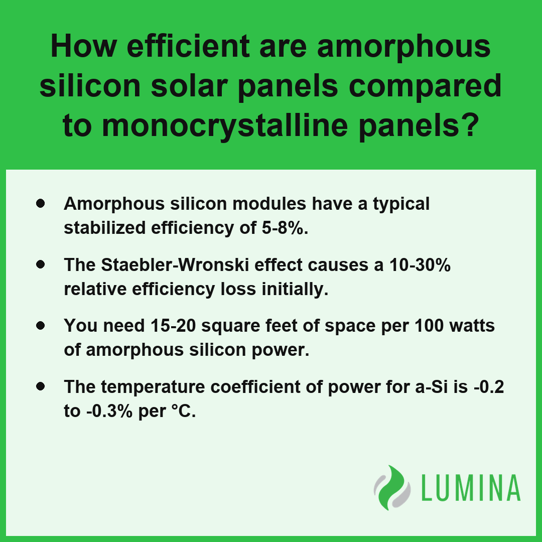
- Amorphous silicon modules have a typical stabilized efficiency of 5-8%.
- The Staebler-Wronski effect causes a 10-30% relative efficiency loss initially.
- You need 15-20 square feet of space per 100 watts of amorphous silicon power.
- The temperature coefficient of power for a-Si is -0.2 to -0.3% per °C.
How Efficient Are Amorphous Silicon Solar Panels Compared to Monocrystalline Panels?
You will find that amorphous silicon thin-film modules typically achieve a stabilized efficiency of 5-8%, which is significantly lower than that of crystalline silicon panels, largely due to a 10-30% relative efficiency loss from the Staebler-Wronski effect during initial sunlight exposure and the inherent constraints of the hydrogenated amorphous silicon (a-Si:H) p-i-n structure.
Solar Module Efficiency Comparison
Lab-Cell Efficiency Versus Commercial Module Efficiency
Amorphous silicon is significantly less efficient than crystalline silicon, typically producing roughly one-third to one-quarter of the output per unit of area. While crystalline silicon modules commonly reach 20-24% efficiency, a-Si products operate at much lower metrics due to the fundamental properties of the material and its p-i-n structure. Because it relies on an intrinsic layer only 0.2-0.5 micrometers thick to collect charge, the internal physics limits total energy conversion compared to thick, high-purity silicon wafers. Per the National Renewable Energy Laboratory, commercial amorphous silicon solar cells typically exhibit conversion efficiencies in the range of 6% to 9%, which remains notably lower than the 15% to 22% range achieved by commercial monocrystalline silicon panels.
Stabilized Efficiency After Initial Light Exposure
When you evaluate these panels, you must distinguish between raw laboratory results and the real-world stabilized efficiency. During the first several hundred hours of sunlight, these modules undergo a 10-30% relative efficiency drop due to the Staebler-Wronski effect before the output levels off.
| Module Type | Efficiency Range |
|---|---|
| Single-junction a-Si | 5-8% |
| Crystalline silicon | 20-24% |
Why a Multijunction (Tandem) Cell Changes the Numbers
To overcome the narrow spectral capture of single-layer hydrogenated amorphous silicon (a-Si:H), manufacturers use a multijunction (tandem) cell design. By stacking a-Si layers with microcrystalline silicon or silicon-germanium, these cells capture a broader segment of the light spectrum. This approach improves the stabilized module efficiency to 8-12%, helping bridge the performance gap while maintaining the benefits of thin-film deposition via plasma-enhanced chemical vapor deposition (PECVD).
Does Lower Efficiency Make Amorphous Silicon a Poor Choice?
No, lower efficiency does not inherently make amorphous silicon a poor choice, as the value of a solar installation depends on your total energy yield rather than peak efficiency alone. While you require 15-20 square feet per 100 watts of installed power, the material’s ability to function effectively at a bandgap of about 1.7-1.8 eV allows it to remain productive where other technologies struggle. Compare the total cost of mounting hardware against the lower weight of thin-film modules to determine if the increased surface area requirement fits your structural constraints.
The performance differences between these technologies are influenced by several specific material and operational characteristics:- Thin-film deposition allows for flexible substrate integration, unlike rigid crystalline wafers.
- Amorphous silicon requires significantly less raw material, resulting in a lower energy payback time.
- The spectral response of amorphous silicon is superior for capturing diffuse or low-light conditions.
- Weight constraints make amorphous silicon more suitable for rooftop applications where structural load is a concern.
Amorphous Silicon Degradation and the Staebler-Wronski Effect
Amorphous silicon degradation is primarily driven by the Staebler-Wronski effect, a phenomenon where the electronic properties of the material change when exposed to intense sunlight. Because amorphous silicon relies on hydrogenated amorphous silicon (a-Si:H) to passivate dangling bonds, the initial exposure to photons creates metastable defects that reduce the material’s conductivity. This process is not a permanent failure of the technology but rather an expected phase in the lifecycle of a thin-film module. According to the American Physical Society, these solar cells typically experience a significant initial decrease in power output during the first few hundred hours of light exposure before reaching a stabilized efficiency level.
| Degradation Metric | Operational Impact Specification |
|---|---|
| Initial Efficiency Decay | 10% to 30% reduction post-fabrication |
| Stabilization Period | First several hundred hours of light exposure |
| Long-term Reliability | Consistent baseline output for 20-25 year lifecycle |
| Thermal Annealing Recovery | Partial defect restoration at 150 °C |
| Manufacturer Rating Standard | Stabilized efficiency (post-degradation) |
Initial Relative Efficiency Loss Range
The magnitude of this transition can be categorized by the following impact on performance:
- Initial relative efficiency loss: 10-30% within the first several hundred hours of sunlight exposure.
- Stabilization: The power output reaches a baseline level and remains consistent for the remainder of the module’s 20-25 year typical power output warranty.
- Reversibility: Heating the material to about 150 °C can induce annealing, which partially repairs the lattice defects and restores some of the lost performance.
Manufacturers account for this drop by rating their thin-film modules based on their stabilized efficiency rather than the higher, temporary output observed immediately after fabrication. This ensures that the wattage you see on the label reflects the long-term reality of the product rather than its factory-fresh peak.
Verify the specific stabilized power rating on the manufacturer’s data sheet to ensure you are sizing your system based on the post-degradation output.
Factors influencing the severity of the Staebler-Wronski effect include the following:- Doping concentration levels within the amorphous silicon layers.
- Intrinsic impurity density, specifically oxygen and carbon contamination.
- Thickness of the active silicon thin-film layer.
- Intensity and spectral distribution of the incidental light source.
- Ambient operating temperature during the stabilization phase.
Amorphous Silicon Performance in Shade, Overcast Weather, and Indoor Light
Amorphous silicon performance in shade, overcast weather, and indoor light remains robust because the material possesses a wider bandgap of about 1.7-1.8 eV, allowing it to respond more effectively to the blue-green portion of the visible light spectrum. While crystalline silicon struggles when light intensity drops or becomes diffused, the inherent spectral sensitivity of a-Si allows it to maintain a higher portion of its nominal output under less-than-ideal sky conditions. Because these modules rely on thin-film layers that are only 0.2-0.5 micrometers thick, they exhibit a unique ability to capture photons in low-light environments that typically fail to trigger significant electron flow in thicker wafer-based counterparts.
| Operational Environment | a-Si Spectral Response Characteristic | Performance Outcome vs. Crystalline Silicon |
|---|---|---|
| Overcast/Cloudy Sky | Blue-Green Wavelength Absorption | Superior energy yield under scattered, diffused photons |
| Artificial/Indoor Lighting | Wide Bandgap (1.7–1.8 eV) Efficiency | Higher conversion rate in low-intensity lux conditions |
| Partial Shading | Thin-Film Surface Uniformity | Maintains electron flow despite localized obstruction |
| Low-Light Intensity | 0.2–0.5 Micron Layer Sensitivity | Enables power generation where thick wafers fail |
- Diffuse light sensitivity: Excellent performance in overcast conditions where sunlight is scattered by clouds rather than hitting the module directly.
- Spectral advantage: Superior conversion of short-wavelength (blue-green) light compared to crystalline silicon, which favors the red-infrared end of the spectrum.
- Indoor applications: High efficiency under low-intensity, artificial lighting sources, making it a preferred choice for small electronic devices and calculators. Per the U.S. Department of Energy, these materials maintain higher conversion efficiencies under low-intensity indoor and artificial light than conventional silicon wafer technologies.
- Partial shade tolerance: Ability to continue generating meaningful power when only portions of the thin-film module surface receive direct illumination.
Observe the specific spectral response charts provided by the manufacturer to match the expected light conditions of your installation site with the frequency sensitivity of the module.
Key advantages of amorphous silicon in non-standard lighting conditions include:- Enhanced temperature coefficients minimize voltage drops during the thermal stress often associated with cloudy, high-humidity environments.
- Reduced material volume requires significantly less energy during the manufacturing process compared to energy-intensive silicon wafer crystallization.
- Flexible substrate compatibility allows for integration onto non-planar surfaces, capturing light from wider incident angles than rigid panels.
- Minimized sensitivity to the “photon drag” effect allows for more consistent power output during rapid fluctuations in light availability.
Amorphous Silicon Versus Crystalline Silicon in Hot Weather
Amorphous silicon outperforms crystalline silicon in hot weather because it exhibits a superior temperature coefficient of power, meaning it loses less efficiency as surface temperatures rise. While crystalline silicon panels suffer significant voltage drops in extreme heat, a-Si maintains a more stable output, making it a reliable option in high-temperature environments. Per Sandia National Laboratories, crystalline silicon panels experience a notable reduction in voltage as cell temperatures rise, whereas amorphous silicon structures maintain greater efficiency stability across high-temperature fluctuations.
Power Loss per °C (Absolute Value)
| Performance Metric | Amorphous Silicon | Crystalline Silicon |
|---|---|---|
| Temperature Coefficient of Power | -0.2 to -0.3% per °C | -0.3 to -0.4% per °C |
| Primary Composition | Hydrogenated amorphous silicon (a-Si:H) | Silicon wafers |
| Deposition Method | PECVD (150-250 °C) | Ingot slicing |
Because the temperature coefficient of power measures the specific percentage drop in output for every degree of heating, the lower absolute value of a-Si allows you to retain a higher percentage of the module’s nameplate wattage on the hottest days of the year. This resilience is inherent to the material properties of hydrogenated amorphous silicon (a-Si:H), which does not experience the same degree of thermal-related electronic mobility degradation found in crystalline structures. When planning your installation, compare the temperature coefficients on product data sheets to estimate how much actual power your modules will retain during peak summer afternoon temperatures.
Selecting the right solar technology requires considering these practical installation factors for high-heat regions:- Prioritize thin-film a-Si deployments for building-integrated photovoltaics (BIPV) where surface temperatures often exceed ambient air levels due to limited ventilation.
- Account for the lower initial conversion efficiency of a-Si by allocating a larger total surface area to meet specific energy production targets compared to crystalline alternatives.
- Leverage the flexible form factor of amorphous modules to install solar arrays on non-traditional, curved surfaces that cannot support rigid crystalline wafers.
- Evaluate site-specific irradiance patterns to determine if the superior low-light performance of a-Si compensates for its lower peak power density during cloudier days.
How Much Roof Space You Need for a Given Wattage of Amorphous Silicon Panels
The roof space you need for a given wattage of amorphous silicon panels is significantly higher than that required for crystalline silicon, typically demanding 15-20 square feet per 100 watts of power capacity. Because amorphous silicon has a lower conversion efficiency, you must account for a larger physical footprint to reach your desired energy production goals. This spatial requirement is a direct result of the thin-film module design, which prioritizes material economy and substrate versatility over the high-density energy output of traditional wafers. Per the United States Department of Energy, the reduced energy density of amorphous silicon compared to crystalline alternatives requires larger installation footprints to achieve high-capacity power outputs in residential or commercial rooftop applications.
| Module Technology | Surface Area Needed (per 1kW System) | Relative Spatial Efficiency | Weight-to-Area Characteristic |
|---|---|---|---|
| Amorphous Silicon (Thin-Film) | 150–200 Square Feet | Low (Baseline) | Ultra-lightweight |
| Crystalline Silicon (Wafer) | 60–80 Square Feet | High (2.5x density) | Standard/Heavy |
Roof Space Required for 1kW System (Sq Ft)
When calculating your installation requirements, you should consider the following comparative footprint demands based on a standard 1-kilowatt (1,000 watt) system:
- Amorphous silicon modules: 150-200 square feet of surface area.
- Crystalline silicon modules: 60-80 square feet of surface area.
- Physical ratio: Amorphous silicon requires roughly 2.5 times the surface area for equivalent power.
Because the light-absorbing intrinsic layer is only 0.2-0.5 micrometers thick, these modules remain extremely lightweight despite the larger total area they occupy on your mounting surface. You should carefully measure the unobstructed, sun-facing square footage of your roof to ensure it can accommodate the wider array dimensions required for an amorphous silicon system.
Consider these secondary factors when evaluating roof capacity for thin-film installations:- Structural Load: The lower weight per square foot of amorphous silicon often allows for installation on roof structures that cannot support the dead load of heavy crystalline racks.
- Surface Irregularities: Thin-film modules offer greater installation flexibility on curved or non-standard architectural surfaces where rigid crystalline panels cannot be mounted.
- Shading Tolerance: Amorphous cells maintain higher relative performance in diffuse light or partial shading conditions, potentially offsetting the need for the larger footprint in sub-optimal locations.
Frequently Asked Questions
What is the p-i-n structure of an amorphous silicon solar cell and why is the layer so thin?
The p-i-n structure of an amorphous silicon solar cell consists of a thin doped p-layer, a thick intrinsic layer, and an n-layer, designed because short carrier diffusion lengths require an internal electric field to collect charge. The intrinsic layer is very thin, typically 0.2-0.5 micrometers, due to strong light absorption.
How is hydrogenated amorphous silicon made for solar panels using PECVD and silane?
Hydrogenated amorphous silicon (a-Si:H) is made via plasma-enhanced chemical vapor deposition (PECVD) by exposing substrates to silane gas and hydrogen at temperatures of about 150-250 °C. This process creates a thin film where hydrogen passivates dangling bonds, allowing the material to be doped and conduct electricity for solar energy capture.
Can amorphous silicon solar panels be flexible, and are they good for RVs, boats, and curved roofs?
Yes, amorphous silicon solar panels can be flexible because they are deposited as thin films onto substrates such as plastic or stainless steel. This flexibility makes them suitable for non-flat applications like RVs, boats, and curved roofs, allowing for installation on surfaces where rigid crystalline silicon wafers cannot be used.
What is amorphous silicon used for in solar, and why is it now a niche product?
Amorphous silicon is used for small consumer electronics like pocket calculators and specialized modules, but it is a niche product because its commercial module efficiency is only 5-8%. Crystalline silicon reaches 20-24% efficiency, requiring significantly less space, which makes amorphous silicon less competitive for large-scale rooftop solar energy installations.
What warranty do amorphous silicon solar panels carry, and are they environmentally safe?
Thin-film a-Si modules typically carry a 20-25 years power output warranty. They are safe to use, though they do experience the Staebler-Wronski effect, which causes a 10-30% relative efficiency drop during initial light exposure before stabilizing. These systems offer an alternative to crystalline silicon for specific low-light applications using amorphous silicon.