
Thin Film Silicon: Cost, Efficiency, Types, Applications, Low-light Performance, Degradation, Thickness, Flexibility and Weight, Manufacturing Process, Lifespan and Warranty
Thin film silicon is a solar cell material made by depositing very thin silicon layers onto glass, metal, or plastic. Key aspects include efficiency, cost, applications, types, degradation, low-light performance, flexibility and weight, thickness, lifespan and warranty, and manufacturing process. The layers are often only a few micrometers thick, which is far less than the wafers used in crystalline panels, so you use much less raw material per panel. Sunlight is absorbed in the silicon, freeing electrons that flow through contacts to produce direct current. Within solar panels, this technology fills a niche for lightweight, flexible, and low-light modules, and you may see it in both amorphous and microcrystalline forms. When you research installers, solar companies Delaware may offer several panel technologies, and thin film silicon is one of the less common options. The article explains efficiency, types, degradation, cost, and applications in turn.
Key Takeaways
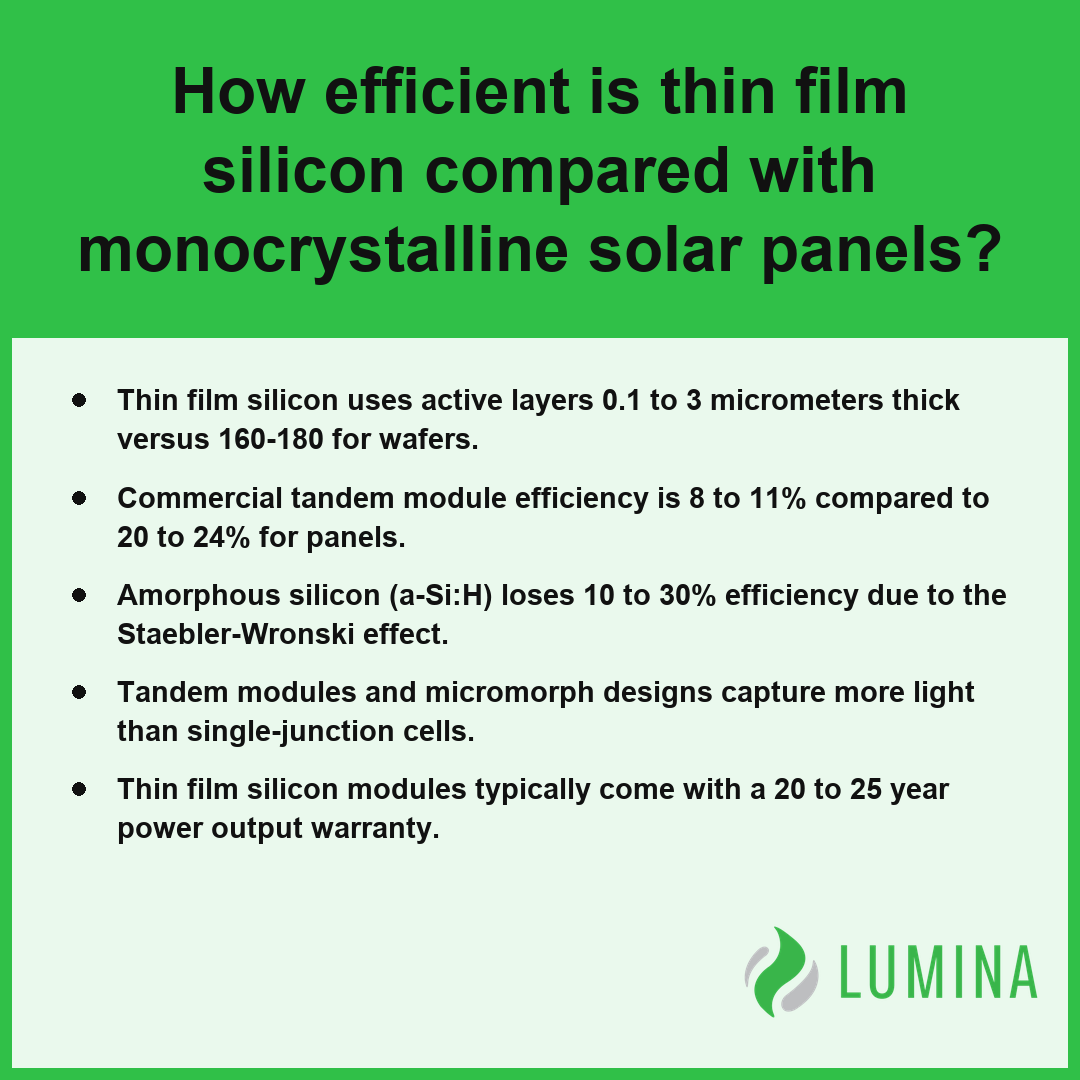
- Thin film silicon uses active layers 0.1 to 3 micrometers thick versus 160-180 for wafers.
- Commercial tandem module efficiency is 8 to 11% compared to 20 to 24% for panels.
- Amorphous silicon (a-Si:H) loses 10 to 30% efficiency due to the Staebler-Wronski effect.
- Tandem modules and micromorph designs capture more light than single-junction cells.
- Thin film silicon modules typically come with a 20 to 25 year power output warranty.
How Efficient Is Thin Film Silicon Compared with Monocrystalline Solar Panels?
Thin film silicon is generally less efficient than monocrystalline solar panels, typically requiring two to three times the total surface area to generate an equivalent amount of electricity. While a crystalline silicon panel commonly achieves a module efficiency between 20 and 24%, thin film silicon modules occupy a much lower performance tier. Because the active layer of thin film silicon is only about 0.1 to 3 micrometers thick—compared to roughly 160 to 180 micrometers for a crystalline silicon wafer—the material absorbs light differently and operates at lower baseline power densities.
Temperature Coefficient of Power (% degradation per °C)
| Technology Type | Typical Module Efficiency |
|---|---|
| Single-junction amorphous silicon (a-Si:H) | 6 to 8% |
| Tandem thin film silicon module | 8 to 11% |
| Crystalline silicon panel | 20 to 24% |
| Multijunction lab-record cells | 14 to 15% (stabilized) |
Despite this disparity in area efficiency, you should evaluate the total footprint available at your site before dismissing the technology. While crystalline silicon panels dominate in power-to-space metrics, thin film silicon maintains a superior temperature coefficient of power, measuring about -0.2 to -0.3% per °C, compared to roughly -0.3 to -0.4% per °C for wafer silicon. Per the National Renewable Energy Laboratory, this thin-film technology is known for a lower temperature coefficient, which results in less efficiency degradation than monocrystalline panels when exposed to the high heat conditions frequently found throughout the United States. This means thin film silicon output holds up more effectively during periods of high ambient heat.
Calculate the exact square footage of your mounting surface and compare it against the expected total energy yield rather than focusing solely on panel-level efficiency percentages.
Consider these additional functional characteristics when weighing thin film silicon against crystalline alternatives:- Weight: Thin film modules are significantly lighter and more flexible, making them suitable for structures with limited load-bearing capacity.
- Shadow Tolerance: Thin film silicon often exhibits better performance under partial shading conditions compared to the series-connected architecture of traditional wafer cells.
- Installation Cost: The monolithic integration process used in manufacturing thin film can lead to lower balance-of-system costs for large-scale deployments.
- Light Sensitivity: These modules typically demonstrate improved performance in diffuse or low-light conditions, such as early morning or overcast weather.
What Are the Different Types of Thin Film Silicon, from Amorphous to Micromorph Tandem?
The different types of thin film silicon are categorized by their crystalline structure and layer composition, which dictate how they capture sunlight and determine their stabilized efficiency. Manufacturers use plasma-enhanced chemical vapor deposition (PECVD) at temperatures of 150 to 250 °C to create these varied material configurations on flexible or rigid substrates.
| Thin Film Silicon Type | Bandgap (eV) | Primary Spectral Focus | Commercial Efficiency (%) |
|---|---|---|---|
| Amorphous (a-Si:H) | 1.7 – 1.8 | Visible Light | 6 – 8 |
| Microcrystalline (µc-Si:H) | 1.1 | Red & Near-Infrared | N/A (Layer Component) |
| Micromorph Tandem | 1.1 – 1.8 (Stacked) | Full Spectrum (Blue to NIR) | 8 – 11 |
Commercial Module Efficiency (%)
- Amorphous silicon (a-Si:H): This material lacks long-range atomic order and relies on hydrogen (about 10% atomic content) to passivate dangling bonds. It features a bandgap of 1.7 to 1.8 eV, allowing an active layer under 1 micrometer to capture significant visible light despite its low commercial module efficiency of about 6 to 8%.
- Microcrystalline silicon (µc-Si:H): By introducing crystalline regions, this variant achieves a lower bandgap of approximately 1.1 eV. This allows it to absorb the red and near-infrared spectrum more effectively than purely amorphous forms, making it a critical component for layering.
- Micromorph tandem modules: These units combine amorphous silicon (a-Si:H) and microcrystalline silicon (µc-Si:H) into a single stack. This tandem approach leverages the strengths of both materials to boost commercial module efficiency to 8 to 11% and enables record laboratory cells to reach roughly 14 to 15% stabilized efficiency. Per the Department of Energy, these tandem cells work by pairing an amorphous top layer for high-energy blue light with a microcrystalline bottom layer to capture low-energy red and infrared light, thereby increasing overall spectral sensitivity.
Because thin film silicon relies on a p-i-n structure—where a thin doped p-layer and n-layer surround a thick intrinsic absorber—you should evaluate whether the specific stacking configuration of the module matches your local solar irradiance spectrum.
The following considerations are essential for the industrial application of thin-film silicon technologies:- Light-Induced Degradation: Amorphous layers experience the Staebler-Wronski effect, causing a decrease in stabilized efficiency during initial sunlight exposure.
- Substrate Flexibility: These materials are compatible with lightweight polymer or thin metal foils, enabling integration into building-integrated photovoltaics (BIPV).
- Thermal Budget: Low-temperature processing (below 250 °C) allows the use of low-cost, flexible substrates that cannot withstand high-temperature crystalline silicon manufacturing.
- Light Trapping Schemes: Textured transparent conductive oxide (TCO) layers are frequently utilized to increase optical path length and improve photon absorption within the thin active layers.
Does Thin Film Silicon Degrade Faster, and What Is the Staebler-Wronski Effect?
Thin film silicon degrades faster than a crystalline silicon panel because the Staebler-Wronski effect causes an initial efficiency loss of about 10 to 30% in amorphous silicon (a-Si:H) active layers during the first several months of light exposure before reaching a stabilized efficiency.
Estimated Initial Efficiency Loss Range
What Causes the Staebler-Wronski Effect in Amorphous Silicon (a-Si:H)?
The Staebler-Wronski effect is a phenomenon where amorphous silicon (a-Si:H) experiences a light-induced reduction in conductivity and performance shortly after installation. Because amorphous silicon (a-Si:H) contains approximately 10% hydrogen to passivate dangling bonds, the atomic structure remains disordered. When exposed to sunlight, these bonds can break, creating metastable defects that hinder electron flow. According to Sandia National Laboratories, the extent of this light-induced degradation is influenced by the thickness of the intrinsic layer, as thinner cells undergo less total degradation because they require shorter carrier collection distances.
How Much Initial Efficiency Is Lost Before Stabilization?
You should anticipate that thin film silicon will lose about 10 to 30% of its initial efficiency in the first several months of light exposure before reaching its stabilized efficiency. Manufacturers account for this drop when rating their modules, so the power output listed on the data sheet represents the stabilized value rather than the untested factory state.
- Amorphous silicon (a-Si:H): Metastable defect formation in hydrogenated bonds.
- Initial degradation: 10 to 30% drop during the first few months.
- Recovery: None; this is a permanent shift to the stabilized efficiency state.
How Does Thin Film Silicon Handle Heat and Long-Term Wear?
Thin film silicon handles heat more effectively than crystalline silicon panels because it possesses a more favorable temperature coefficient of power. While crystalline silicon panels suffer significantly as temperatures rise, thin film silicon maintains its performance under intense solar radiation.
| Technology | Temperature Coefficient (%/°C) |
|---|---|
| Thin film silicon | -0.2 to -0.3 |
| Crystalline silicon panel | -0.3 to -0.4 |
What Do Power Output Warranties Tell You?
Power output warranties for thin film silicon modules typically span about 20 to 25 years. These agreements cover the expected output based on the panel’s stabilized efficiency, ensuring that the module does not degrade beyond predefined levels after the initial light-induced transition. Evaluate the degradation rate specified in the warranty documentation to determine how the power output will shift over the second and third decade of your installation.
Factors that influence the severity of the Staebler-Wronski effect include:- Light Intensity: Higher levels of irradiance accelerate the formation of metastable defects.
- Temperature: Elevated operating temperatures can facilitate the annealing process, potentially mitigating some defect accumulation.
- Material Purity: Impurities such as oxygen or carbon within the silicon network can increase the density of defect sites.
- Deposition Technique: The method of plasma-enhanced chemical vapor deposition determines the initial hydrogen distribution and structural disorder of the film.
Thin Film Silicon vs. Crystalline Silicon Panels: Cost Once Installation and Area Are Counted
Thin film silicon vs. crystalline silicon panels: cost once installation and area are counted depends largely on the balance between material savings and the footprint required for energy parity. While thin film silicon uses significantly less raw material, its lower module efficiency compared to crystalline silicon panels necessitates more mounting hardware, cabling, and structural support to achieve the same total power output. Per Lawrence Berkeley National Laboratory, the total installed cost of solar energy systems is increasingly influenced by soft costs like permitting, labor, and hardware overhead, which can disproportionately impact thin-film systems due to their need for more expansive mounting configurations.
Module Efficiency (%)
| Metric | Thin Film Silicon | Crystalline Silicon Panels |
|---|---|---|
| Active layer thickness | 0.1 to 3 micrometers | 160 to 180 micrometers |
| Module efficiency | 6 to 11% | 20 to 24% |
| Area needed for same power | 2 to 3 times higher | Baseline (1x) |
| Temperature coefficient of power | -0.2 to -0.3% per °C | -0.3 to -0.4% per °C |
The economic trade-off centers on the land or roof area available. Because you need a significantly larger surface area to capture the same energy as a high-efficiency crystalline silicon panel, installation costs for racking and labor can often negate the savings realized from the thinner, less material-intensive silicon layers. However, in environments with extreme heat, the superior temperature coefficient of power of thin film silicon may reduce long-term operational losses compared to crystalline alternatives. Evaluate your specific available installation footprint versus the total system capacity needed to determine if the area-to-cost ratio favors a larger, lower-efficiency array or a compact, high-efficiency system.
The following factors often dictate when thin-film technology remains a viable alternative to crystalline silicon despite its lower efficiency:- Weight-sensitive surfaces: Thin-film panels are ideal for roofs with low structural load-bearing capacity where heavy crystalline modules cannot be installed.
- Flexible applications: The thin, lightweight nature of these cells allows for integration onto curved surfaces or non-traditional building envelopes.
- Low-light and diffuse light performance: Thin-film materials often maintain higher energy production during cloudy or overcast conditions compared to traditional panels.
- High-heat environments: The superior temperature coefficient allows for less energy degradation in extremely hot climates where efficiency drops occur in standard modules.
What Thin Film Silicon Is Used for Today and Whether It Suits a Home Roof
Thin film silicon is primarily used today in specialized applications where lightweight, flexible, or aesthetic integration is required, and it often suits a home roof only under specific structural or design constraints. Because it uses an active layer of only about 0.1 to 3 micrometers compared to the 160 to 180 micrometers required for a crystalline silicon wafer, it can be deposited on thin metal foils or plastics that conform to non-traditional surfaces. According to the United States Department of Energy, amorphous silicon thin-film technology is generally relegated to building-integrated photovoltaics or niche industrial uses instead of typical residential arrays because of its lower power density. However, since commercial module efficiency typically sits between 6 and 8% for single-junction amorphous silicon (a-Si:H) and 8 to 11% for tandem modules, you must account for the significant surface area required to match the output of a crystalline silicon panel.
| Thin Film Technology Variant | Module Efficiency Range | Primary Application Focus | Substrate Requirement |
|---|---|---|---|
| Single-junction (a-Si:H) | 6% – 8% | Aesthetic/Architectural Integration | Metal Foil or Polymer Plastic |
| Tandem Modules | 8% – 11% | BIPV and Flexible Portable Power | Lightweight/Flexible Substrate |
Typical Module Efficiency (%)
- Building-integrated photovoltaics (BIPV): These modules serve as roofing shingles or facade elements that replace traditional building materials rather than sitting on top of them.
- Portable and flexible power: Due to the low-temperature plasma-enhanced chemical vapor deposition (PECVD) process (150 to 250 °C), these panels are produced on lightweight substrates ideal for camping gear or emergency power kits.
- Large-scale aesthetic installations: Thin film silicon offers a uniform, dark appearance that is often preferred by architects for projects where the grid-like look of crystalline silicon panels is considered undesirable.
- High-heat environments: With a temperature coefficient of power of about -0.2 to -0.3% per °C, these modules perform more reliably in extreme heat than standard wafer-based alternatives.
Compare the total usable square footage of your roof against the required power density to determine if the lower conversion efficiency of these modules leaves you with enough capacity to meet your energy goals.
Consider these key factors when evaluating thin-film silicon for potential installation:- Assess the available surface area, as the lower power density necessitates a larger footprint to achieve equivalent energy yields compared to crystalline silicon.
- Verify the structural weight capacity of the mounting surface to determine if the lightweight nature of thin-film materials offers a distinct advantage for your specific project.
- Evaluate the aesthetic requirements of the building envelope, as these modules can be integrated directly into glass facades or non-standard roofing geometries.
- Review the local climate conditions, as thin-film variants typically demonstrate better performance stability in high-temperature environments than traditional crystalline panels.
Frequently Asked Questions
How thin is thin film silicon compared with a standard crystalline silicon solar wafer?
Thin film silicon has an active silicon layer thickness of about 0.1 to 3 micrometers, which is significantly thinner than the roughly 160 to 180 micrometers required for a crystalline silicon wafer. This substantial reduction in material volume is possible because amorphous silicon (a-Si:H) absorbs light very strongly.
Does thin film silicon work better in shade, cloudy weather, or hot conditions than regular solar panels?
Yes, thin film silicon works better in these conditions because its temperature coefficient of power is about -0.2 to -0.3% per °C, which is milder than the -0.3 to -0.4% per °C found in crystalline silicon panels. It also offers superior performance during diffuse light and cloudy weather.
How is thin film silicon made using plasma-enhanced chemical vapor deposition?
Thin film silicon is made using plasma-enhanced chemical vapor deposition (PECVD) by reacting silane and hydrogen gas at low temperatures of about 150 to 250 °C. This process allows the deposition of the p-i-n structure onto inexpensive substrates like glass, metal foil, or plastic to create the active layer.
How light and flexible are thin film silicon solar panels, and can they fit a curved roof?
Thin film silicon panels are highly versatile and flexible because the active layer is deposited on lightweight substrates such as metal foil or plastic rather than rigid wafers. This physical composition allows the modules to conform to curved surfaces, provided the installation surface supports the underlying flexible or thin-glass material.
How long do thin film silicon solar panels last, and what do their warranties cover?
Thin film silicon solar panels generally last 20 to 25 years, with typical power output warranties covering the same 20 to 25 year duration. Manufacturers rate these modules at the stabilized efficiency, accounting for the 10 to 30% power loss experienced during the initial months due to the Staebler-Wronski effect.