
Nanometers: Cutoff Wavelength, Light Wavelengths, Size, Coating Thickness, Cell Color, Photon Energy, Performance Impact, Layer Thickness, Nanostructures, Energy Split
Nanometers are units of length equal to one billionth of a meter, used to measure light wavelengths and thin layers. Key aspects include light wavelengths, cutoff wavelength, coating thickness, size, photon energy, cell color, layer thickness, performance impact, energy split, and nanostructures. In solar panels, nanometers describe the wavelengths of sunlight that cells absorb, from about 300 nm in the ultraviolet to roughly 1,100 nm in the near infrared for silicon. Silicon has a cutoff wavelength near 1,100 nm, because photons beyond it carry too little energy to free an electron. Photon energy rises as wavelength shrinks, so shorter wavelengths deliver more energy, though any excess is lost as heat. Anti-reflective coatings are often about 70 to 80 nm thick, a size tuned so that reflected light cancels out and more sunlight enters the cell. Specifications from solar installers DC often reference these figures when describing how a panel responds to different parts of the solar spectrum, and the sections below explain size, wavelength, cutoff, photon energy and coating thickness in turn.
Key Takeaways
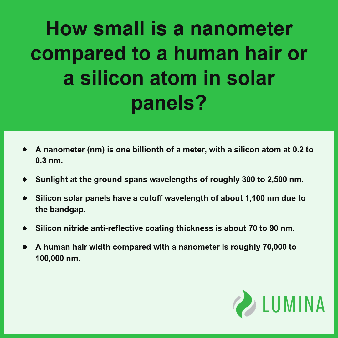
- A nanometer (nm) is one billionth of a meter, with a silicon atom at 0.2 to 0.3 nm.
- Sunlight at the ground spans wavelengths of roughly 300 to 2,500 nm.
- Silicon solar panels have a cutoff wavelength of about 1,100 nm due to the bandgap.
- Silicon nitride anti-reflective coating thickness is about 70 to 90 nm.
- A human hair width compared with a nanometer is roughly 70,000 to 100,000 nm.
How Small Is a Nanometer (nm) Compared to a Human Hair or a Silicon Atom?
A nanometer (nm) is a unit of length equal to one billionth of a meter, a scale so minuscule that thousands of these units can fit across the width of a single human hair. According to the National Nanotechnology Initiative, a single nanometer is approximately 100,000 times smaller than the diameter of an average human hair. To understand this dimension, consider that a nanometer (nm) represents the basic increment used to engineer modern electronic materials, where physical dimensions determine how light interacts with matter.
Scale Comparisons in Nanometers (nm)
Nanometers Versus a Human Hair
While a human hair spans roughly 70,000 to 100,000 nm in width, the structures engineered for solar energy harvesting often operate at a fraction of that size. This extreme scale allows engineers to manipulate surface properties and light absorption at the atomic level.
What Is the Scale of a Silicon Atom in a Crystalline Silicon Wafer?
At the foundation of a crystalline silicon wafer, individual silicon atoms measure only about 0.2 to 0.3 nm across. Because these atoms define the material’s internal structure, the spacing between them dictates the electrical properties of the solar cell.
Why Quantum Dot Size Is Measured in Nanometers
The performance of advanced materials like quantum dots, which are about 2 to 10 nm across, is governed entirely by their physical size. By controlling their dimensions in nanometers, researchers tune the exact wavelength of light these crystals can absorb.
Layer Thicknesses Measured in Nanometers
Different solar technologies utilize vastly different layer thicknesses, ranging from thin coatings to structural wafers. The following table compares these dimensions:
| Component | Typical Thickness (nm) |
|---|---|
| Silicon Nitride Coating | 70 to 90 |
| Perovskite Cell | 300 to 600 |
| CIGS Thin-Film | 1,000 to 2,000 |
| Cadmium Telluride Absorber | 1,500 to 3,000 |
| Crystalline Silicon Wafer | 150,000 to 180,000 |
Compare the thickness of your specific cell type against the wavelength of the light it is designed to capture to understand how effectively it might trap photons.
The following list highlights how manipulating material dimensions at the nanometer scale influences solar energy technology:- Bandgap tuning: Changing the size of quantum dots shifts the specific range of the solar spectrum they can absorb.
- Surface-to-volume ratio: Decreasing structural size increases the reactive surface area, enhancing catalytic efficiency in photo-electrochemical cells.
- Light trapping: Nanostructured textures on cell surfaces reduce reflection by effectively “bending” incoming light into the absorber layer.
- Charge carrier mobility: Precisely engineered atomic spacing minimizes internal resistance, allowing electrons to travel through the material with fewer collisions.
Which Nanometer Wavelengths of Sunlight Do Solar Panels Actually Use?
The nanometer (nm) wavelengths of sunlight that solar panels actually use range from roughly 300 nm to 2,500 nm, though each specific cell technology selectively harvests only a portion of this spectrum. While sunlight reaching the ground spans this entire broad range, crystalline silicon cells are restricted by their bandgap, limiting their effective absorption primarily to the visible and near-infrared regions. Per the National Renewable Energy Laboratory, photons shorter than 300 nm are mostly filtered by the atmosphere or glass, while those exceeding 1,200 nm generally lack the energy required to produce electron-hole pairs in silicon. Other materials like perovskite cells can be tuned to capture different parts of the spectrum, which is why researchers often combine them with silicon to process light that would otherwise be wasted. Beyond these primary materials, specialized components like quantum dots allow for even more precise harvesting of specific wavelengths.
| Spectral Region | Wavelength Range (nm) | Silicon Photovoltaic Interaction | Energy Utility |
|---|---|---|---|
| Ultraviolet | 300 – 380 | Minimal; mostly filtered or lost | Primarily converted to heat |
| Visible | 380 – 750 | High absorption | Primary driver of electron-hole pairs |
| Near-Infrared | 750 – 1,100 | Functional absorption limit | Secondary contribution to current |
| Extended Infrared | 1,100 – 2,500 | Transparent; lacks bandgap energy | Wasted (requires tandem materials) |
Upper Wavelength Limit of Solar Spectrum Regions (nm)
- Ultraviolet: 300 to 380 nm (mostly higher energy, often converted to heat)
- Visible: 380 to 750 nm (primary driver of conventional cell efficiency)
- Near-Infrared: 750 to 1,100 nm (the functional limit for crystalline silicon)
- Extended Infrared: 1,100 to 2,500 nm (largely passes through standard silicon wafers)
When you evaluate potential solar technologies, consider how effectively a module’s specific material composition matches the incoming sunlight distribution at your installation site.
Beyond the basic spectral interactions, several external factors influence the practical efficiency of these photovoltaic conversions:- Angle of Incidence: Sunlight striking the panel at non-perpendicular angles increases reflection losses, effectively reducing the intensity of available photons.
- Thermal Degradation: As panels heat up due to absorbed non-productive wavelengths, the crystalline silicon’s voltage output decreases, lowering overall conversion efficiency.
- Surface Texturing: Manufacturers apply anti-reflective coatings and pyramid-shaped textures to silicon wafers to “trap” light, increasing the path length of photons and boosting absorption probability.
- Atmospheric Conditions: Particulates, humidity, and cloud cover selectively scatter shorter wavelengths, altering the spectral distribution that reaches the cell surface throughout the day.
Why Silicon Solar Panels Cannot Use Light Above 1,100 Nanometers
Silicon solar panels cannot use light above 1,100 nanometers because the energy contained in these long-wavelength photons is insufficient to displace electrons within the semiconductor’s atomic structure. Crystalline silicon has a bandgap of approximately 1.12 eV, which functions as an energetic threshold; if a photon’s energy is lower than this value, it lacks the capacity to bridge the bandgap, allowing the light to pass through the material entirely without contributing to the flow of current. Per the American Physical Society, the fundamental optical absorption edge of crystalline silicon is dictated by its electronic band structure, which makes the material transparent to infrared radiation past the 1,100 nanometer threshold. Because photon energy is inversely proportional to its wavelength, any light measuring longer than the 1,100 nanometer cutoff represents a wasted transmission that cannot be converted into electricity.
Photon Wavelength Limits (Nanometers)
The relationship between photon wavelength and the ability of a material to absorb that energy determines the effective spectrum for a solar cell. The following table illustrates how specific regions of the electromagnetic spectrum interact with the silicon lattice:
| Wavelength Range | Interaction with Silicon |
|---|---|
| 300 to 750 nanometers | High absorption, significant energy excess converted to heat |
| 750 to 1,100 nanometers | Efficient absorption, closer to the 1.12 eV bandgap ideal |
| Above 1,100 nanometers | Zero electrical contribution; photons pass through the cell |
Observe the spectral sensitivity charts provided by manufacturers to understand how your specific panel captures light across this infrared boundary.
Beyond the spectral absorption limits, several secondary factors influence the electrical output of silicon cells:- Thermal degradation reduces voltage as semiconductor temperatures rise during operation.
- Reflective losses occur at the cell surface, requiring anti-reflective coatings to maximize light entry.
- Internal resistance within the silicon lattice and metal contacts causes additional energy dissipation.
- Shading from grid lines prevents light from reaching the underlying photoactive material.
How Wavelength in Nanometers Determines Photon Energy and Efficiency Limits
How wavelength in nanometers determines photon energy and efficiency limits is dictated by a fixed inverse relationship where shorter wavelengths carry higher energy. Because photon energy in electron volts (eV) is calculated by dividing approximately 1240 by the wavelength in nanometers, each individual photon hitting your solar panel must possess enough energy to overcome the material’s bandgap to create an electrical current. When photons have wavelengths shorter than the bandgap threshold, they contain excess energy that is inevitably wasted as heat, which significantly restricts the theoretical conversion efficiency of single-junction solar cells to roughly 33%.
| Light Segment | Wavelength Range (nm) | Photon Energy Impact | Contribution to Efficiency |
|---|---|---|---|
| Ultraviolet | < 380 | Excessively high | High thermal waste |
| Visible | 380 – 750 | Optimal | Primary current generation |
| Near-Infrared | 750 – 1,100 | Marginal | Approaching excitation limit |
| Infrared/Beyond | > 1,100 | Insufficient | Zero current contribution |
Wavelength Range of Light Segments (nm)
You can understand the relationship between specific light segments and their contribution to efficiency by observing how different energy levels interact with silicon:
- Ultraviolet light (below 380 nm): Carries high photon energy, but produces substantial waste heat.
- Visible light (380 to 750 nm): Provides the primary contribution to electrical current generation.
- Near-infrared light (750 to 1,100 nm): Contains lower photon energy, approaching the limit for successful electron excitation.
- Light above 1,100 nm: Lacks the energy required to excite electrons, resulting in zero current contribution.
Per the Department of Energy, it is understood that photons with wavelengths longer than 1,100 nanometers carry insufficient energy to create electron-hole pairs in silicon, causing this infrared radiation to pass through the cell without being converted into electricity.
Consider the trade-off between heat generation and current output when evaluating how much of the spectrum your specific solar panel design effectively converts into usable electricity.
Beyond the fundamental interactions with silicon, several secondary factors further influence the conversion efficiency of solar cells:- Reflection losses: Photons that bounce off the panel surface rather than being absorbed are lost, necessitating anti-reflective coatings.
- Recombination rates: Electrons excited by photons can fall back into the valence band before reaching the external circuit, dissipating energy as heat.
- Shading effects: Physical obstructions, such as metal contact fingers on the cell surface, prevent light from reaching the semiconducting material.
- Resistance losses: The internal electrical resistance of the cell leads to voltage drops as the current flows toward the electrodes.
How Thick Is an Anti-Reflective Coating on a Solar Panel in Nanometers?
The anti-reflective coating on a solar panel is typically about 70 to 90 nanometers (nm) thick. According to the National Renewable Energy Laboratory, these coatings are generally engineered to a thickness of approximately 70 to 100 nm to minimize light reflection through destructive interference. This precise thickness is essential because it is engineered to be a quarter of the wavelength of light near 600 nm, causing destructive interference that minimizes the amount of light bouncing off the cell surface. By applying a layer of silicon nitride at this scale, manufacturers successfully cut reflection from roughly 30% to under 5%. Because these thin layers are so sensitive to light interference, variations of just 10 to 20 nm in the coating thickness can cause the panel to shift in visible color, often resulting in the dark blue appearance you see on many standard modules.
Light Reflection Percentage
| Property | Value or Impact |
|---|---|
| Silicon nitride thickness | 70 to 90 nm |
| Reflection reduction | From 30% to under 5% |
| Color sensitivity | 10 to 20 nm change alters appearance |
Observe the uniform color across a module’s surface to judge the consistency of its anti-reflective coating thickness.
Beyond the core optical mechanics, the manufacturing process maintains panel efficiency through these secondary considerations:- Uniform vapor deposition rates are maintained across the silicon wafer to prevent batch-level color inconsistencies.
- The refractive index of the silicon nitride must be precisely matched to the silicon substrate to ensure optimal light trapping.
- Quality control inspections utilize spectrophotometry to verify the destructive interference range across the entire surface area.
- Environmental sealing is required to protect the thin-film layer from long-term chemical degradation or moisture ingress.
Frequently Asked Questions
How much of the sun’s energy is visible light, infrared, or ultraviolet in nanometer terms for solar panels?
Roughly 40-50% of solar energy at the surface is visible light (380-750 nm), about 50% is infrared (above 750 nm), and under 5% is ultraviolet (below 380 nm). Sunlight reaching the ground spans a total range of roughly 300 to 2,500 nm to power solar panels.
Why do solar cells look dark blue or black, and what do nanometers have to do with it?
Solar cells look dark blue because their silicon nitride anti-reflective coating, roughly 70 to 90 nm thick, interferes with light waves to reduce reflection. This thickness cuts surface reflection from roughly 30% to under 5%, and a variation of just 10-20 nm in this measurement shifts the visible color.
Why can thin-film solar layers work at only a few hundred to a few thousand nanometers thick?
Thin-film solar layers work at these thicknesses because they use materials that absorb photons efficiently without needing the bulk of a crystalline silicon wafer. For instance, cadmium telluride absorbers are about 1,500 to 3,000 nm thick, while perovskite cell layers are typically only 300 to 600 nm thick.
What are quantum dots, plasmonic particles, and black silicon, and how do their nanometer sizes affect solar cells?
Quantum dots are semiconductor crystals about 2 to 10 nm across that absorb specific wavelengths based on their size, while plasmonic metal particles at 20-100 nm concentrate light, and black silicon uses nanoscale surface features to trap light and minimize reflection to improve total solar cell light absorption.
Do nano-coatings measured in nanometers really make solar panels more efficient?
Yes, nano-coatings measured in nanometers significantly improve solar panel efficiency by drastically reducing light reflection. By applying a silicon nitride anti-reflective coating of about 70 to 90 nm, you lower the reflected light from roughly 30% to under 5%, ensuring more energy enters the cell for power conversion.