
Thin Film: Types, Efficiency, Lifespan, Price, Space Needs, Heat Tolerance, Materials Safety, Flexibility and Weight, Applications, Thickness
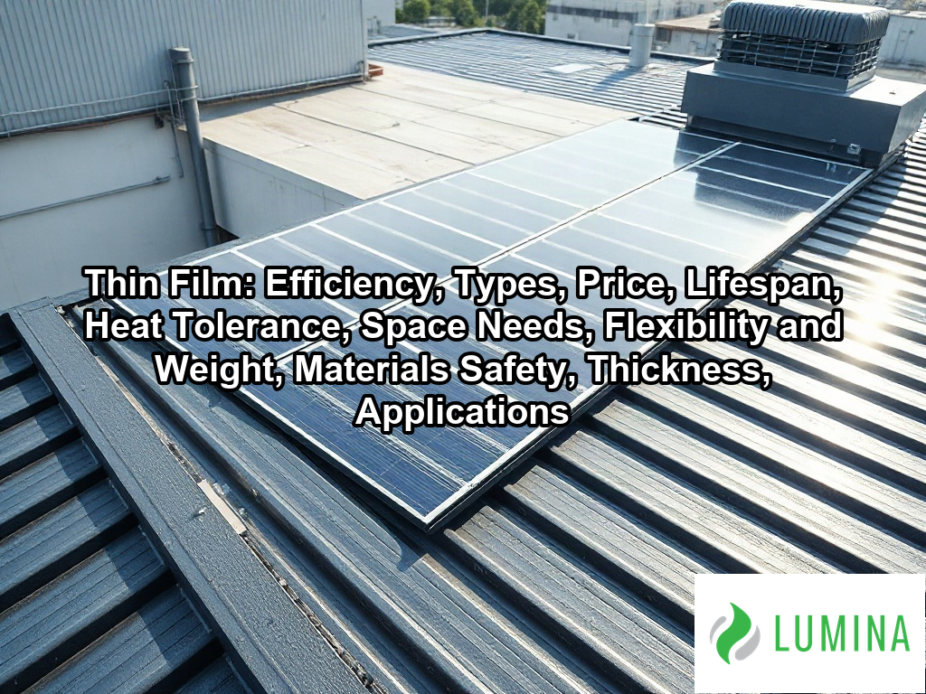
A thin film solar panel is a photovoltaic module made by depositing ultra-thin semiconductor layers onto glass, plastic, or metal. Key aspects include efficiency, types, price, lifespan, heat tolerance, space needs, flexibility and weight, materials safety, thickness, and applications. Each layer absorbs sunlight and releases electrons, which creates an electric current you can use in a building or send to the grid. Within the solar industry, these modules offer a lighter and more flexible alternative to traditional silicon wafer designs, though they usually convert less sunlight per square foot. If you are researching solar panels Washington DC, you will find that roof space, shading, and seasonal weather all influence how this technology performs. The article goes on to explain efficiency, the main types such as cadmium telluride and amorphous silicon, typical price ranges, expected lifespan, and how these modules handle high temperatures.
Key Takeaways
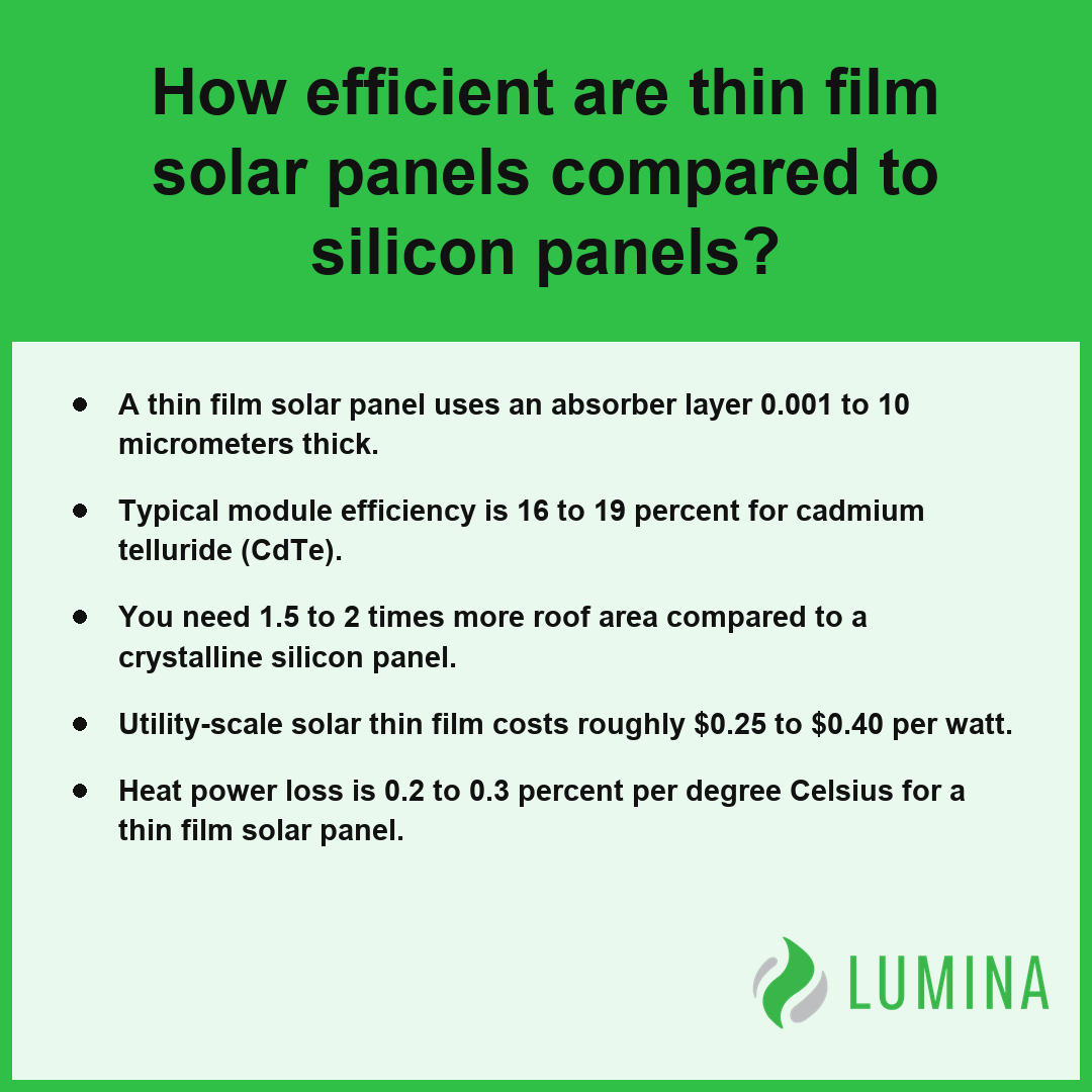
- A thin film solar panel uses an absorber layer 0.001 to 10 micrometers thick.
- Typical module efficiency is 16 to 19 percent for cadmium telluride (CdTe).
- You need 1.5 to 2 times more roof area compared to a crystalline silicon panel.
- Utility-scale solar thin film costs roughly $0.25 to $0.40 per watt.
- Heat power loss is 0.2 to 0.3 percent per degree Celsius for a thin film solar panel.
How Efficient Are Thin Film Solar Panels Compared to Silicon Panels?
You will find that a thin film solar panel generally offers lower module efficiency of 16 to 19 percent compared to 20 to 24 percent for a crystalline silicon panel, though you may benefit from a superior temperature coefficient of 0.2 to 0.3 percent per degree Celsius when selecting cadmium telluride (CdTe), copper indium gallium selenide (CIGS), amorphous silicon (a-Si), or perovskite technologies. Lawrence Berkeley National Laboratory reports that thin film solar technologies often exhibit lower temperature coefficients than silicon, allowing for more stable power output in the high-heat conditions frequently found in many regions of the United States.
Typical Commercial Module Efficiency
Module Efficiency by Absorber Layer Material
A thin film solar panel generally offers lower module efficiency than a crystalline silicon panel, with commercial variants typically converting 6 to 19 percent of sunlight into electricity compared to the 20 to 24 percent conversion rate found in mainstream crystalline silicon panels.
| Technology | Commercial Module Efficiency |
|---|---|
| Cadmium telluride (CdTe) | 16 to 19 percent |
| Copper indium gallium selenide (CIGS) | 13 to 17 percent |
| Amorphous silicon (a-Si) | 6 to 10 percent |
| Crystalline silicon panel | 20 to 24 percent |
Why Lab Records Differ From Commercial Modules
Laboratory environments often yield significantly higher performance metrics than mass-produced hardware. While best-in-class research cells have demonstrated perovskite-on-silicon tandem efficiencies exceeding 33 percent, technical hurdles in stabilizing these materials for outdoor exposure mean commercial production remains focused on more reliable, lower-efficiency absorber layer chemistries.
Does Lower Efficiency Matter for Your Roof?
Yes, lower efficiency matters for your roof because it dictates the physical footprint required to meet your energy goals. Because the absorber layer in a thin film solar panel is less dense in its energy output than silicon, you may need roughly 1.5 to 2 times the total surface area to generate the same kilowatt capacity. This spatial requirement is the primary reason this technology is common for expansive utility-scale solar installations but rarely seen on residential rooftops where space is restricted. When calculating your potential yield, measure your total available roof square footage against the lower power density of thin film to ensure your design footprint remains viable.
Key physical characteristics that distinguish thin-film solar technologies from crystalline silicon include:- Physical Profile: Thin-film modules are lightweight and flexible, making them suitable for installations where roof loading capacity is limited.
- Aesthetics: These panels typically feature a uniform, dark appearance that is often preferred for building-integrated photovoltaics (BIPV).
- Shading Tolerance: Thin-film materials generally demonstrate superior performance under partial shading conditions due to their circuit design.
- Manufacturing Process: Unlike silicon wafers, these panels are produced by depositing photovoltaic layers onto substrates like glass, plastic, or metal, allowing for continuous roll-to-roll production.
Types of Thin Film Solar Panels: CdTe, CIGS, Amorphous Silicon and Perovskite
Types of thin film solar panels are categorized by their specific semiconductor absorber layer, which typically measures between 0.001 to 10 micrometers in thickness to capture sunlight and generate current. These materials are deposited onto substrates like glass, plastic, or stainless steel using high-precision manufacturing processes such as vapor transport or sputtering to create a lightweight, continuous semiconductor surface.
| Thin Film Material | Commercial Module Efficiency | Laboratory Peak Potential | Primary Application / Characteristic |
|---|---|---|---|
| Cadmium telluride (CdTe) | 16% – 19% | Not specified | Utility-scale; high material recovery |
| Copper indium gallium selenide (CIGS) | 13% – 17% | ~23% | Complex absorber layer |
| Amorphous silicon (a-Si) | 6% – 10% | Not specified | Flexible laminate structures |
| Perovskite | Emerging | >26% (Single) / >33% (Tandem) | Rapidly advancing crystal structure |
Typical Commercial Module Efficiency (%)
- Cadmium telluride (CdTe): The dominant commercial technology for utility-scale solar, providing a robust module efficiency of 16 to 19 percent with a highly efficient material recovery process that captures over 90 percent of the semiconductor content.
- Copper indium gallium selenide (CIGS): A technology featuring a complex absorber layer that reaches laboratory efficiencies near 23 percent, typically resulting in commercial module efficiencies of 13 to 17 percent.
- Amorphous silicon (a-Si): A version of thin film that uses non-crystalline silicon to create modules, offering a lower commercial efficiency of 6 to 10 percent but benefiting from manufacturing compatibility with flexible laminate structures.
- Perovskite: An emerging category defined by its crystal structure, capable of exceeding 26 percent efficiency in laboratory single-junction cells and surpassing 33 percent when integrated into tandem cell designs with silicon. According to the Department of Energy, while these materials have shown rapid gains in power conversion efficiency in research settings, they still need more durability testing to ensure they can withstand long-term outdoor use across the United States.
Evaluate the specific durability and recycling profile of the semiconductor material chosen for your installation before finalizing your hardware selection.
Thin film solar technologies offer distinct operational advantages beyond their efficiency ratings:- Environmental Resilience: High tolerance to heat compared to traditional crystalline silicon, maintaining stable performance in high-temperature environments.
- Low-Light Performance: Superior energy harvesting capabilities during dawn, dusk, or cloudy conditions due to a broader spectral response.
- Bifacial Potential: Capability to be manufactured on transparent substrates, allowing for the generation of electricity from both the front and rear sides.
- Manufacturing Scalability: Suitability for roll-to-roll processing techniques, which can significantly reduce long-term production costs.
What Thin Film Solar Panels Cost Per Watt
The cost of a thin film solar panel at the utility-scale level generally ranges from roughly $0.25 to $0.40 per watt. Because these modules are manufactured using continuous, automated production lines—employing vapor transport, sputtering, or solution coating processes—they require significantly less semiconductor material than a crystalline silicon panel. With semiconductor layers typically ranging from 0.001 to 10 micrometers thick, these panels utilize roughly 1/100 or less of the raw material found in traditional silicon wafers, which helps keep the baseline manufacturing costs lower for large-scale installations.
| Metric | Specification / Value |
|---|---|
| Utility-Scale Price Range | $0.25 – $0.40 per watt |
| Semiconductor Layer Thickness | 0.001 – 10 micrometers |
| Material Utilization Ratio | <1% of crystalline silicon mass |
| CdTe Recycling Efficiency | >90% material recovery rate |
| Primary Production Method | Continuous automated vapor/sputter coating |
Thin Film Solar Cost per Watt (USD)
When you evaluate the total capital expenditure for a system, consider how these pricing structures break down across different project scales and material types:
- Utility-scale thin film solar panel market price: $0.25 to $0.40 per watt.
- Material savings: Less than 1/100 of the semiconductor mass compared to crystalline silicon.
- Manufacturing advantage: Automated, high-speed continuous production lines.
- Recycling value: Established recovery programs that reclaim over 90 percent of the semiconductor material in cadmium telluride (CdTe) modules.
Before committing to a specific procurement strategy, calculate the balance of system expenses, as the larger installation footprint required for lower-efficiency modules may offset the initial savings gained from a lower price per watt. According to the Solar Energy Industries Association, while thin film technologies often feature lower price points per watt at the manufacturing level, the total installed cost in the United States market is significantly influenced by balance-of-system expenses such as racking, labor, and land-use requirements.
When planning large-scale deployments, consider these additional factors that influence project viability:- Operational temperature coefficients for thin-film modules typically outperform crystalline silicon in high-heat environments.
- Installation logistics benefit from lighter module weight, which can reduce mounting structure and ballast requirements.
- Geographic flexibility is increased by the lower degradation rates of thin-film modules when exposed to partial shading or diffuse light.
- End-of-life management is simplified by established take-back programs that facilitate the recovery of rare semiconductor components.
Lifespan and Power Degradation of Thin Film Solar Panels
The lifespan and power degradation of a thin film solar panel generally align with industry standards, typically offering a linear power output warranty of 25 to 30 years. Like other photovoltaic technologies, these panels experience a gradual reduction in output over time due to environmental exposure and chemical changes within the semiconductor materials. Per the National Renewable Energy Laboratory, thin-film modules often exhibit an initial power degradation of 2% to 5% during the first year of operation before stabilizing. You can expect an annual degradation rate of about 0.5 to 1 percent per year, which reflects the gradual stabilization of the absorber layer following initial installation.
Estimated Annual Power Degradation Rate (%)
Factors influencing the long-term reliability of your array include the specific semiconductor composition and the encapsulation methods used to protect the layers from moisture and oxidation. Because these modules are often manufactured in continuous, automated lines, the consistency of the deposition process plays a significant role in determining how well a thin film solar panel maintains its output levels throughout its operational life. The following table outlines key reliability metrics to consider when evaluating the longevity of these systems:
| Metric | Standard Expectation |
|---|---|
| Linear power output warranty | 25 to 30 years |
| Annual degradation rate | 0.5 to 1 percent per year |
| Material recovery (CdTe) | Over 90 percent via recycling |
Confirm that the manufacturer provides a robust end-of-life recycling plan to ensure the semiconductor materials are reclaimed at the conclusion of the warranty period.
To maximize the long-term reliability and performance of your thin-film solar array, consider these maintenance and environmental factors:- Perform periodic visual inspections to check for seal integrity and edge corrosion, which can compromise moisture protection.
- Ensure the mounting structure allows for proper thermal expansion to prevent mechanical stress on the thin-film layers.
- Monitor inverter performance logs to distinguish between standard module degradation and localized shading or soil accumulation.
- Maintain a documented cleaning schedule using non-abrasive materials to prevent micro-scratches on the protective glass or polymer front sheet.
Thin Film Solar Panels vs. Silicon Panels in Heat and Shade
Thin film solar panels generally outperform crystalline silicon panels when operating in high-temperature environments or areas prone to partial shading. Because the thin film semiconductor layers are significantly thinner—ranging from 0.001 to 10 micrometers—they demonstrate a superior temperature coefficient, meaning they maintain voltage stability more effectively as the ambient air heats up. According to the National Renewable Energy Laboratory, thin-film solar modules generally exhibit lower temperature coefficients than crystalline silicon, which means they experience a smaller decline in power output as ambient temperatures rise.
Power Loss Per Degree Celsius (Percentage)
| Performance Metric | Thin Film Solar Panel | Crystalline Silicon Panel |
|---|---|---|
| Power loss per degree Celsius | 0.2 to 0.3 percent | 0.3 to 0.4 percent |
| Shade tolerance | High (strip-based design) | Low (cell-level impact) |
| Thermal performance | Better in extreme heat | Standard |
The primary advantage in heat stems from the semiconductor material’s inherent physical properties, which allow the thin film solar panel to experience less efficiency drop-off than its silicon counterpart. Furthermore, thin film designs often utilize long, narrow strips for their internal circuitry. If debris or a structure casts a shadow across a portion of the array, only the directly affected strips lose output, whereas the series-connected architecture of a typical crystalline silicon panel can cause the power production of an entire string to drop significantly. Evaluate your local average daytime temperatures and the presence of persistent tree or chimney shadows to determine if the thermal and shading resilience of thin film justifies the additional roof space required for installation.
Thin film solar panels offer several additional installation and structural advantages:- Reduced structural load requirements due to the lightweight, flexible nature of the semiconductor materials.
- Enhanced architectural versatility for installation on curved or non-traditional roof surfaces.
- Lower carbon footprint during the manufacturing process compared to energy-intensive crystalline silicon production.
- Ability to integrate into building-integrated photovoltaics (BIPV) for aesthetic and functional surface coverage.
Frequently Asked Questions
How thin is a thin film solar cell and why does it use so little semiconductor material?
A thin film solar cell uses a semiconductor layer that is 0.001 to 10 micrometers thick. Because this is roughly 1/100 or less of the material required for a 150 to 200 micrometer thick crystalline silicon panel, the manufacturing process achieves significant material savings through highly efficient, automated deposition lines.
How much more roof space do thin film solar panels need for a home?
A residential system needs roughly 1.5 to 2 times the roof area of a crystalline silicon panel system. This requirement exists because typical module efficiency is lower, ranging from 16 to 19 percent for cadmium telluride (CdTe), compared to 20 to 24 percent for mainstream crystalline silicon panels.
Can thin film solar panels bend, and are they light enough for roofs that can’t hold heavy panels?
Yes, thin film solar panels can bend when manufactured as a flexible laminate, which can weigh under 2 pounds per square foot. These lightweight versions are ideal for structures with limited load-bearing capacity, offering a practical alternative to the heavier, rigid construction of a standard crystalline silicon panel.
Is the cadmium in thin film solar panels dangerous, and can the panels be recycled?
Yes, the cadmium in thin film solar panels is managed through recycling programs that recover over 90 percent of the semiconductor material in cadmium telluride (CdTe) modules. These established industry programs ensure that modules are processed safely at the end of their 25 to 30 year linear power output warranty.
What are thin film solar panels used for besides solar farms?
Beyond utility-scale solar, thin film is used in space and specialty applications where gallium arsenide thin film serves high-performance needs. Its ability to perform well in diffuse light or partial shading also makes specific configurations of thin film useful for diverse environments where traditional panels may face significant installation challenges.